
Unusual electronic structure of Dirac material BaMnSb2 revealed by angle-resolved photoemission spectroscopy?
2021-06-26 03:04:32HongtaoRong戎洪濤LiqinZhou周麗琴JunbaoHe何俊寶ChunyaoSong宋春堯YuXu徐煜YongqingCai蔡永青CongLi李聰QingyanWang王慶艷LinZhao趙林GuodongLiu劉國東ZuyanXu許祖彥GenfuChen陳根富HongmingWeng翁紅明andXingjiangZhou周興江
Chinese Physics B 2021年6期
關鍵詞:趙林
Hongtao Rong(戎洪濤) Liqin Zhou(周麗琴) Junbao He(何俊寶) Chunyao Song(宋春堯)Yu Xu(徐煜) Yongqing Cai(蔡永青) Cong Li(李聰) Qingyan Wang(王慶艷)Lin Zhao(趙林) Guodong Liu(劉國東) Zuyan Xu(許祖彥) Genfu Chen(陳根富)Hongming Weng(翁紅明) and Xingjiang Zhou(周興江)
1National Laboratory for Superconductivity,Beijing National Laboratory for Condensed Matter Physics,Institute of Physics,Chinese Academy of Sciences,Beijing 100190,China
2University of Chinese Academy of Sciences,Beijing 100049,China
3Henan International Joint Laboratory of MXene Materials Microstructure,College of Physics and Electronic Engineering,
Nanyang Normal University,Nanyang 473061,China
4Songshan Lake Materials Laboratory,Dongguan 523808,China
5Technical Institute of Physics and Chemistry,Chinese Academy of Sciences,Beijing 100190,China
6Beijing Academy of Quantum Information Sciences,Beijing 100193,China
Keywords: ARPES,BaMnSb2,Dirac material,magnetic topological material
Topological materials, including topological insulators,topological semimetals, and topological superconductors,have attracted much attention due to their unique electronic structure, exotic physical properties, and potential applications.[1–7]Magnetic topological materials,with the introduction of magnetism to break the time-reversal symmetry,can generate novel topological phases such as the quantum anomalous Hall state.[8–15]TheAMnPn2(A=Ca, Sr, Ba, Eu or Yb;Pn=Bi or Sb)family has provided a desirable platform to search for intrinsic magnetic topological materials.[16–26]In these materials, the Bi or Sb layer can host Dirac dispersion and the Mn sublattice can provide magnetic environment. The introduction of Eu or Yb on theAsite can further manipulate the magnetic structure in the system. In addition to the magnetic structure,it has been found that the electronic structure and topological properties also depend sensitively on the crystal structure.[27]Among all the compounds in theAMnPn2family, BaMnSb2is unique because it has a crystal structure that is distinct from other members in the family. While there have been some investigations on BaMnSb2,[21,24,28–30]the detailed study of its electronic structure is still limited.[21,24]
In this paper, we have carried out detailed high resolution angle resolved photoemission spectroscopy (ARPES)measurements and band structure calculations to study the electronic structure of BaMnSb2. The observed Fermi surface mainly consists of one hole pocket aroundΓand a strong spot atY. The measured band structures are dominated by nearly linear bands that extend to a wide energy range.The measured electronic structures are unusual which deviate obviously from the band structure calculations.
High-quality single crystals of BaMnSb2were grown by flux method.[31]The elements Ba,Mn,and Sb were mixed in the ratio of Ba:Mn:Sb=1:1:4, put into an alumina crucible,and sealed in a quartz tube. The quartz tube was heated slowly to 900?C,held for 20 hours,and then cooled to 700?C at a rate of 1?C/hour,where the excess flux was removed using a centrifuge. Shiny platelike single crystals with a typical dimension of 5×5×1 mm3were obtained. We carried out single crystal x-ray diffraction to analyze the crystal structure of the samples at 273 K. It crystalizes in an orthorhombic structure (space group:Imm2) with lattice constantsa=24.258 ?A,b=4.4827 ?A, andc=4.506 ?A, consistent with the previous reports.[21,24]ARPES measurements were performed at our lab-ARPES system equipped with 21.218 eV Helium discharge lamp and Scienta DA30L electron energy analyzer.[32,33]The energy resolution was set at~20 meV.The angular resolution was~0.3?. The Fermi level is referenced by measuring on the Fermi edge of a clean polycrystalline gold that is electrically connected to the sample. All the samples were cleavedin situand measured in ultrahigh vacuum with a base pressure better than 5×10?11mbar.
The first-principle calculations to simulate the electronic structures of BaMnSb2were implemented by using the Viennaab initiosimulation package(VASP).[34]The generalized gradient approximation (GGA) of the Perdew–Burke–Ernzerhof(PBE)type was selected to describe the exchange–correlation function.[35]The Brillouin zone(BZ)integration was sampled by 3×11×11kmesh and the cut-off energy was set to 500 eV.Spin–orbital coupling (SOC) was taken into account. The tight-binding model of BaMnSb2was constructed by using the Wannier90 with Ba 5d orbitals,Sb 5p orbitals,and Mn 3d orbitals, which is based on the maximally-localized Wannier functions(MLWF).[36]The bulk Fermi surfaces of BaMnSb2were calculated by the WannierTools package.[37]
The crystal structure of BaMnSb2is shown in Fig.1(a).It consists of an alternate stacking of MnSb4layer and Ba–Sb–Ba layer along theaaxis. In the central Ba–Sb–Ba layer, the Sb atoms in the Sb sheet form zig-zag chains with the chain direction along thebaxis (Fig. 1(b)). The Ba atoms above and below the Sb sheet are coincident. Figure 1(c) shows the measured Fermi surface mapping of BaMnSb2at 30 K.The main features observed consist of a circular Fermi surface sheet aroundΓand a strong spot atY. No features are observed atX. Figure 1(d) shows the constant energy contours at different binding energies. At low binding energies below~100 meV, one circle can be observed aroundΓ. When the binding energy is higher than~200 meV,combined with the detailed band structure analysis nearΓ(Fig. 2) and nearY(Fig.3), three main features appear aroundΓ: an outer sheetα,an inner vertical ellipseβ,and another inner horizontal ellipseγ. With increasing binding energy,the outerαsheet increases in its area significantly while the two inner ellipsesβandγget elongated along their long axis. In the mean time,as seen in Fig.1(d), the feature atYstays as a strong spot up to the binding energy of~200 meV and it disintegrates at higher binding energies.
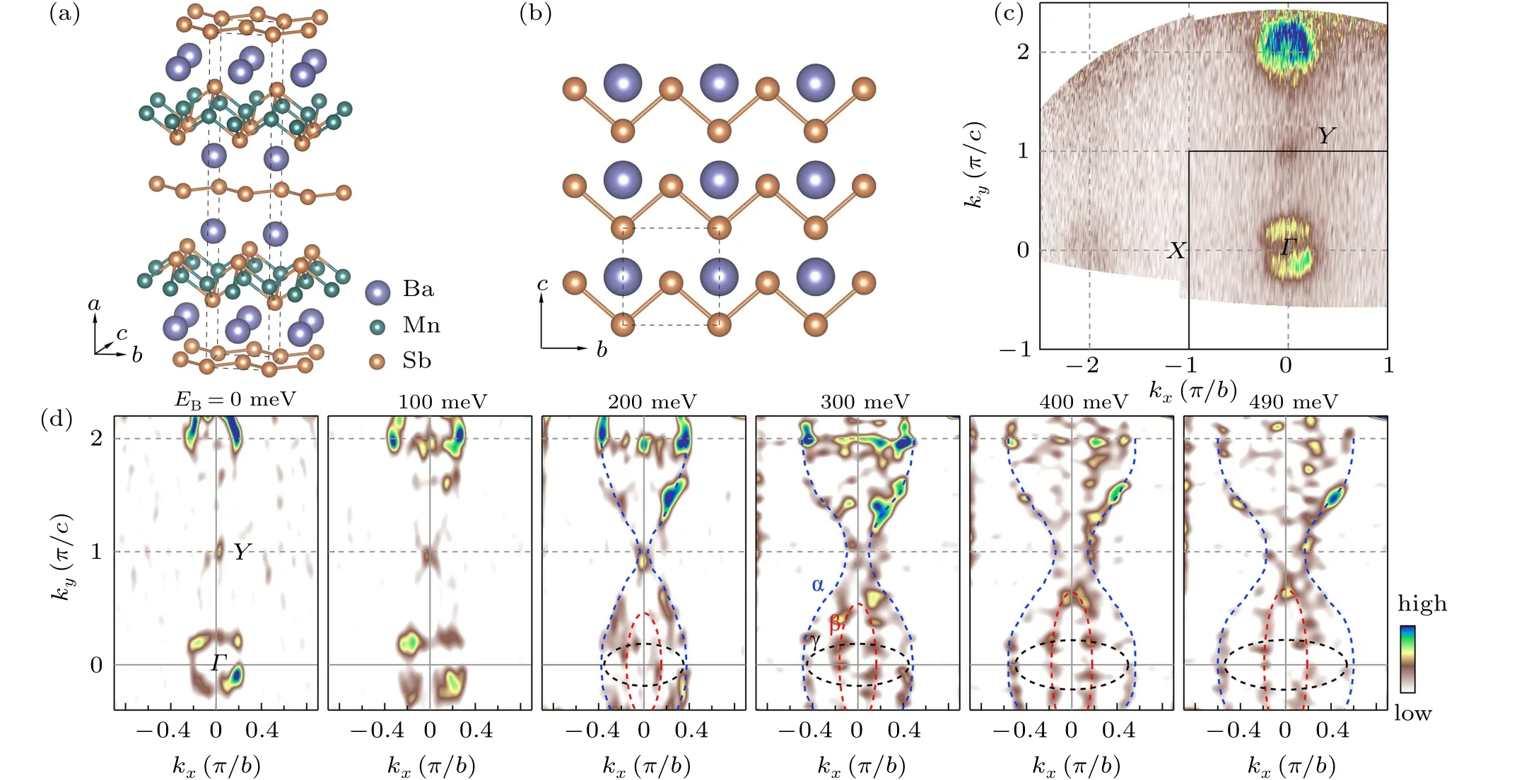
Fig. 1. Fermi surface mapping and constant energy contours of BaMnSb2. (a) Crystal structure of BaMnSb2. The unit cell is indicated by the black dashed lines. (b)Top view of the central Ba–Sb–Ba layer which consists of the zig-zag chainlike structure along the b axis in the Sb layer. (c)Fermi surface mapping obtained by integrating the photoemission spectral weight over a[?20,20]meV energy window with respect to the Fermi level. (d)Constant energy contours at different binding energies of 0 meV, 100 meV, 200 meV, 300 meV, 400 meV, and 490 meV. These are second derivative images obtained by integrating the spectral weight over a[?20,20]meV energy window with respect to each binding energy.
In Fig.2,we zoom in onto the detailed electronic structure aroundΓpoint in BaMnSb2. Figures 2(a)–2(d)show the band structures measured along different momentum cuts aroundΓ. In all these measurements, mainly two sets of bands are observed, labeled asαandβbands in Fig. 2(b) for the cut 6 along theΓ–Xdirection and labeled asβandγbands in Fig.2(d)for the cut 12 along theΓ–Ydirection. Theseα,β,andγbands are nearly linear in dispersion that extend to a wide energy range up to 0.9 eV (Fig. 2(b)). As seen in Figs. 2(a)and 2(b)for the momentum cuts parallel toΓ–X, theβband is very steep; the corresponding Fermi velocity is~13 eV·?A for theβband in Fig. 2(b). The two linear bandsαandβintersect,as shown in Figs.2(a)and 2(b),and the energy position of the crossing point varies for different momentum cuts.For the momentum cuts 4 to 8,we find that the crossing point is closed the Fermi level. These Dirac cone-like bands give rise to the formation of the hole-like Fermi surface aroundΓas shown in Fig.2(e). When the momentum cuts move away further fromΓ(cuts 1–3 and cuts 9–11),the crossing point of theαandβbands shifts down from the Fermi level and the spectral weight at the Fermi level gets depleted. Theαandβbands observed in Fig.2 contribute to the formation of theαandβsheets in the constant energy contours at high binding energies above 200 meV in Fig. 1(d). The band structure for the cut 12 along theΓ–Ydirection, shown in Fig. 2(d), also consists of two main bands aroundΓ. In this case,combined with the constant energy contours in Fig.1(d),the outer band can be assigned toβthat forms theβsheet in Fig.1(d)while the innerγband contributes to the formation of theγsheet in Fig.1(d). In addition to the main linear bandsαandβ,there is another band observed in the measured band structure for the momentum cut 6 along theΓ–Xdirection(Fig.2(c)). This band is flat; it does not show up in the MDC second derivative image in Fig. 2(b) but becomes clear in the EDC second derivative image in Fig. 2(c). The band lies about 130 meV below the Fermi level. The combined MDC and EDC second derivative analyses provide a complete picture of the band structure aroundΓ(Figs.2(a)–2(c)).
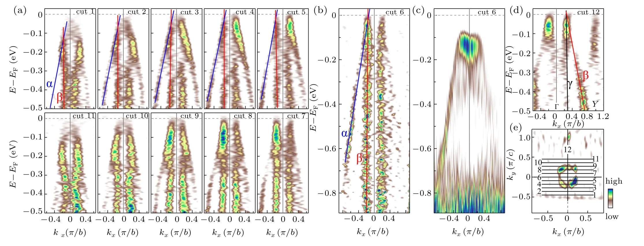
Fig. 2. Hole-like Fermi surface and detailed band structures of BaMnSb2 around Γ measured at 30 K. (a)–(b) Band structure measured along the Γ–X direction for various momentum cuts at different kys. These are the second derivative images with respect to momentum. The location of the momentum cuts,cut 1 to cut 11,is marked by black lines in(e). (c)Band structure for momentum cut 6. It is the second derivative image with respect to energy. (d)Band structure for momentum cut 12; its location is marked by black line in (e). It is the second derivative image with respect to momentum. (e) Fermi surface mapping around Γ. It is the second derivative image obtained by integrating the spectral weight over a[?20,20]meV energy window with respect to the Fermi level.
Figure 3 shows the zoomed-in constant energy contours and the detailed electronic structures of BaMnSb2around theYpoint. In all the bands measured along different momentum cuts aroundYin Figs. 3(d) and 3(e), we observe mainly one set of bands,named asδin Fig.3(e).Theseδbands are nearly linear over a large energy range (~0.9 eV in Fig. 3(e)). For the momentum cut 6 along theY–Mdirection, the two linear bands have a Fermi velocity of~2.9 eV·?A and cross each other near the Fermi level (Fig. 3(e)). When the momentum cuts move away from cut 6 (cut 1 to cut 5 and cut 7 to cut
11 in Fig.3(d)),the spectral weight gets suppressed more and more below the Fermi level. Such a momentum-dependent band evolution produces a strong spot atYin the measured Fermi surface(Fig.3(a))and the evolution of the constant energy contours aroundYas shown in Figs.1(d),3(b),and 3(c).In addition to the main linear bands,there is another band observed in the measured band structure for the momentum cut 6 along theY–Mdirection (Fig. 3(f)). This band is hole-like with its top at~300 meV. It does not show up in the MDC second derivative image in Fig.3(e)but becomes visible in the EDC second derivative image in Fig.3(f).
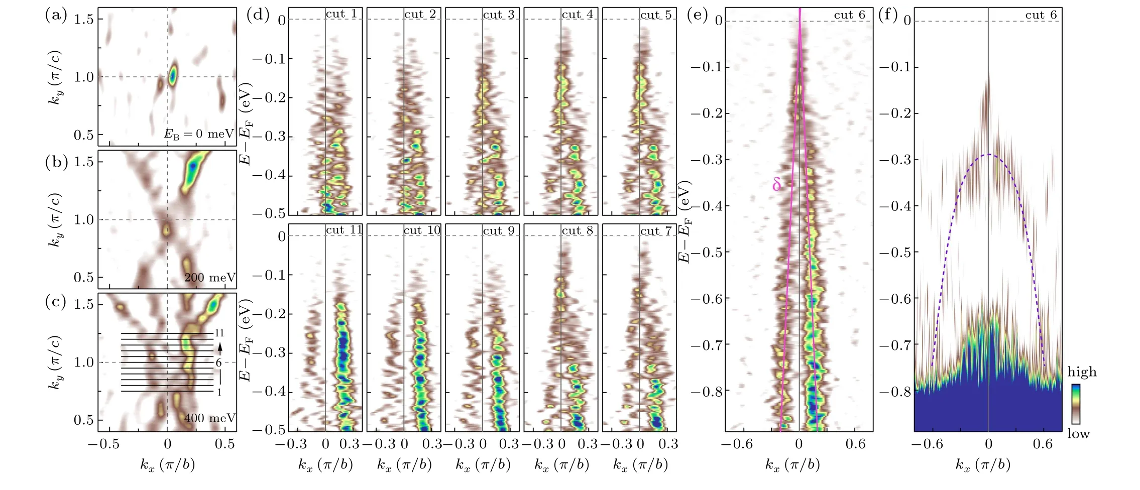
Fig.3. Fermi surface mapping and detailed band structures of BaMnSb2 around Y measured at 30 K.(a)–(c)Constant energy contours at binding energies of 0 meV(a),200 meV(b),and 400 meV(c). These are second derivative images obtained by integrating the spectral weight over a[?20,20]meV energy window at binding energies of 0 meV, 200 meV, and 400 meV. (d)–(e) Band structure measured along the Γ–X direction for various momentum cuts at different kys. These are the second derivative images with respect to momentum. The location of the momentum cuts,cut 1 to cut 11,is marked by black lines in(a). (f)Band structure for momentum cut 6. It is the second derivative image with respect to energy.
In order to understand our measured results, we carried out detailed band structure calculations of BaMnSb2as shown in Fig.4.In the calculations,we took a G-type magnetic structure in BaMnSb2(Fig.4(a))where both the interlayer and intralayer couplings between two nearest moments in the MnSb4layer are antiferromagnetic.[28]Figure 4(c) shows the overall calculated band structure of BaMnSb2without considering the spin–orbital coupling (SOC). The low energy band structure near theΓpoint mainly consists of two M-shaped bands. The band structure near theYpoint is dominated by a cusp structure below the Fermi level and a dip structure above the Fermi level.The position of the cusp and dip structures deviates from theYpoint along theY–Mdirection.Even without considering SOC, there is a prominent gap between the dip and the cusp which is about 380 meV.When SOC is taken into account in the band structure calculations, overall it causes the lifting of the band degeneracy and band splitting as seen in Figs. 4(d)and 4(e). The effect of SOC on the low energy band structure near theΓpoint is small but dramatic changes of the band structure occur near theYpoint(Figs.4(d)and 4(e)). The initial one band of the cusp and dip structures in Fig.4(c)splits into multiple bands. In the meantime, both structures move towards the Fermi level and develop into a Dirac cone-like band with a much reduced gap of~130 meV.The low energy electronic structure of BaMnSb2is rather two-dimensional.Whenkzmoves from 0(Fig.4(d))toπ/a(Fig.4(e)),the bands near theYpoint are barely changed,although there is a slight change in the bands near theΓpoint.
Now we compare the calculated and measured electronic structures of BaMnSb2. Figures 5(a) and 5(b) compare the calculated (Fig. 5(a)) and measured (Fig. 5(b)) band structures along several high symmetry directions. Figures 5(c)–5(f)compare the calculated(Figs.5(c)and 5(d))and measured(Figs. 5(e) and 5(f)) Fermi surface and constant energy contour. Considering the observation of the feature atY, an experimental Fermi levelEF(exp)is taken which is 0.16 eV below the Fermi level in the calculation as show in Fig. 5(a). The measured electronic structure of BaMnSb2shows some consistence with the calculations on a few main aspects. The first is the hole like bands aroundΓand Dirac-like band aroundY(Figs.5(a)and 5(b)).Second,the Fermi surface consists of the hole like sheet aroundΓand some peculiar features aroundY(Figs. 5(c) and 5(e)). Third, the observed features in the measured constant energy contour (Fig. 5(f))) show some resemblance to those in the calculated constant energy contour(Fig. 5(d)). However, the overall calculated electronic structure shows some strong deviations from the measured results.First,the number of the observed bands is much less than that of the calculated bands both around theΓandYpoints. Second,the observed bands are nearly linear that extend to a large energy range of~0.9 eV (Fig. 5(b)). It is hard to find the corresponding bands in the calculations(Fig.5(a)). Third,although there are some similarities in the calculated and measured Fermi surface and constant energy contours, there remain significant differences on the size of the Fermi surface and the features in the constant energy contour. In some other compounds like SrMnBi2,CaMnBi2,and CaMnSb2,the measured electronic structure is found to be in excellent agreement with the band structure calculations.[17,27]The measured electronic structure of BaMnSb2is unusual that it can not be described properly by the band structure calculations.
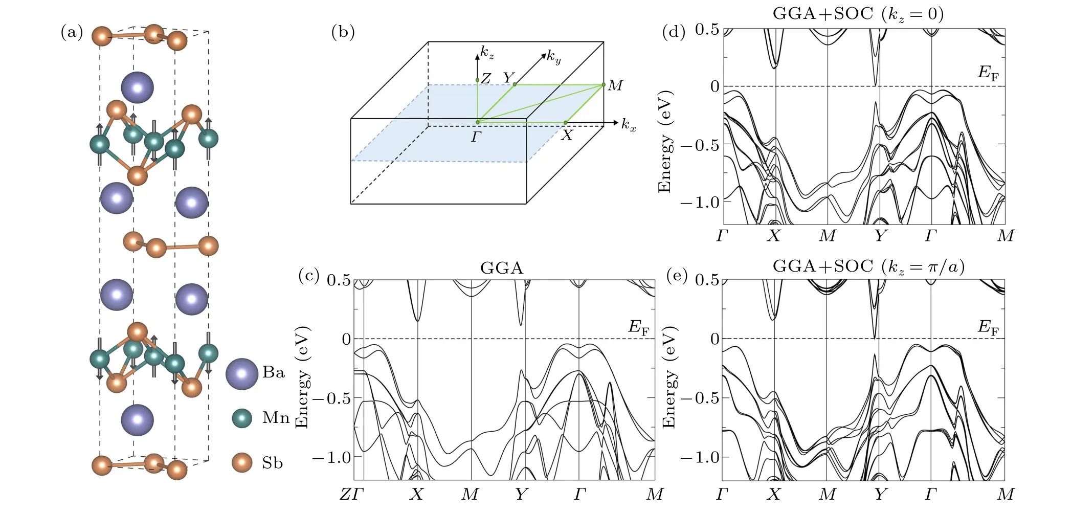
Fig. 4. Calculated band structures of BaMnSb2. (a) Magnetic structure of BaMnSb2. (b) Three-dimensional Brillouin zone of BaMnSb2. Green lines indicate high symmetry directions. (c)–(d)Calculated band structure of BaMnSb2 without(c)and with(d)spin–orbit coupling at kz=0. (e)Calculated band structure with spin–orbit coupling at kz=π/a.
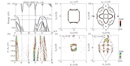
Fig. 5. Comparison between the calculated and measured electronic structures of BaMnSb2. (a) Calculated band structure of BaMnSb2 with spin–orbit coupling at kz=0. (b)Measured band structure of BaMnSb2. This is the second derivative image with respect to the momentum. (c)–(d)Calculated Fermi surface (c) and constant energy contour at a binding energy of 0.3 eV (d). (e)–(f) Measured Fermi surface (e) and constant energy contour at a binding energy of 0.4 eV(f). These are second derivative images obtained by integrating the spectral weight over a[?20,20]meV energy window with respect to each binding energy.
In summary, we have carried out detailed high resolution ARPES measurements and band structure calculations to study the electronic structure of BaMnSb2. The measured electronic structure of BaMnSb2is unusual in three aspects.First, all the measured bands are nearly linear that extend to a wide energy range. Second, the observed Fermi surface mainly consists of one hole pocket aroundΓand a strong spot atY. The Fermi surface is formed from the crossing points of the linear bands. Third, the measured electronic structure deviates strongly from the band structure calculations. These results will stimulate further efforts to theoretically understand the electronic structure of BaMnSb2and search for novel properties in this Dirac material.
猜你喜歡
科普童話·神秘大偵探(2021年7期)2021-09-16 02:47:32
黃河黃土黃種人(2018年9期)2018-11-10 05:11:42
昆崳(2018年2期)2018-10-09 07:42:04
祝你幸?!ぶ?2016年1期)2016-02-17 22:29:50
伴侶(2015年7期)2015-07-16 05:32:56
女士(2015年12期)2015-07-05 07:12:35
分憂(2015年6期)2015-06-09 17:17:24
藍盾(2015年10期)2015-05-30 10:48:04
現代婦女(2014年12期)2014-12-12 04:36:08
婦女生活(2014年9期)2014-09-10 07:22:44

- Chinese Physics B的其它文章
- Coarse-grained simulations on interactions between spectrins and phase-separated lipid bilayers?
- Constraints on the kinetic energy of type-Ic supernova explosion from young PSR J1906+0746 in a double neutron star candidate?
- Computational model investigating the effect of magnetic field on neural–astrocyte microcircuit?
- Gas sensor using gold doped copper oxide nanostructured thin films as modified cladding fiber
- Exact explicit solitary wave and periodic wave solutions and their dynamical behaviors for the Schamel–Korteweg–de Vries equation?
- Suppression of ferroresonance using passive memristor emulator