Hardware Architecture of Polyphase Filter Banks Performing Embedded Resampling for Software-Defined Radio Front-Ends
Mehmood Awan ,Yannick Le Moullec ,Peter Koch ,and Fred Harris
(1.Technology Platforms Section,Dept.of Electronic Systems,Aalborg University,Denmark;
2.Dept.of Electrical&Computer Engineering,San Diego State University,CA,USA)
Abstract In this paper,we describe resource-efficient hardware architectures for software-defined radio(SDR)front-ends.These architectures are made efficient by using a polyphase channelizer that performs arbitrary sample rate changes,frequency selection,and bandwidth control.We discuss area,time,and power optimization for field programmable gate array(FPGA)based architectures in an M-path polyphase filter bank with modified N-path polyphase filter.Such systems allow resampling by arbitrary ratios while simultaneously performing baseband aliasing from center frequencies at Nyquist zones that are not multiples of the output sample rate.A non-maximally decimated polyphase filter bank,where the number of data loads is not equal to the number of M subfilters,processes M subfilters in a time period that is either less than or greater than the M data-load’s time period.We present a load-process architecture(LPA)and a runtime architecture(RA)(based on serial polyphase structure)which have different scheduling.In LPA,N subfilters are loaded,and then M subfilters are processed at a clock rate that is a multiple of the input data rate.This is necessary to meet the output time constraint of the down-sampled data.In RA,M subfilters processes are efficiently scheduled within N data-load time while simultaneously loading N subfilters.This requires reduced clock rates compared with LPA,and potentially less power is consumed.A polyphase filter bank that uses different resampling factors for maximally decimated,under-decimated,over-decimated,and combined up-and down-sampled scenarios is used as a case study,and an analysis of area,time,and power for their FPGA architectures is given.For resource-optimized SDRfront-ends,RA is superior for reducing operating clock rates and dynamic power consumption.RA is also superior for reducing area resources,except when indices are pre-stored in LUTs.
Keyw ords SDR;FPGA;Digital Front-ends;Polyphase Filter Bank;Embedded Resampling
1 Introduction
P olyphase filter banks are versatile engines that perform embedded resampling uncoupled from frequency selection and bandwidth control[1],[2].In a previous paper“Polyphase Filter Banks for Embedded Sample Rate Changes in Digital Radio Front-Ends”[3],we described the benefits of such a polyphase engine.Five embedded resampling approaches were discussed:1)maximally decimated,2)under-decimated,3)over-decimated,and combined up-and down-sampling with 4)single and 5)multiple stride lengths of the commutator(which feeds input data into the filter bank).These are efficient approaches to rational resampling in polyphase filter banks because there is no computational cost,and only a state machine is required to schedule the interactions.Polyphase engines are promising candidates for realizing software-defined radio(SDR)front-ends where embedded sample rate changes are needed.This paper describes the associated hardware architecture designed to reduce area,time,and power consumption of such a polyphase engines implemented on FPGA.
The hardware platform is the most prominent and challenging component of an SDRbecause it must provide massive computationalpower and flexibility at the same time[4],[5].An important semiconductor technology is the field programmable gate array(FPGA).It consists of a vast array of configurable logic blocks,multipliers,and memories,and it allows a custom data path to be tailored to the application at hand.Parallel processing capabilities in an FPGA has made them the core processing engine in SDRapplications.The rich architecture of FPGAwith specialized functionalities allows a large design space.In such a large design space,resource-optimized architectures are highly desirable for implementing SDR functions.In this paper,we describe an FPGA-based architecture for polyphase filter banks that is optimized in terms of area,time,and power.A filter bank performs rational sample rate changes together with frequency control and bandwidth reduction.
In section 2,we analyze five structures for the polyphase filter banks in terms of required resources(referred to as resource complexity)and operating clock rates.From these structures,we select the serial polyphase structure with parallel multiply and accumulate(MAC)and explore its implementation options.In section 3,the selected structure is mapped onto the FPGA in two different implementation architectures that are built on different scheduling.These architectures are called load-process architecture(LPA)and runtime architecture(RA).In section 4,we compare resource usages in the LPAand RAvariants of the five embedded resampling cases in terms of slice registers,slice lookup tables(LUTs),and dedicated resources as well as the operating clock rates.In section 5,we analyze the dynamic power consumed in the LPA and the RAvariants of the five resampling cases.Section 6 concludes the paper.
2 Architecture Design
In this section,we analyze the architectures of the FPGA implementation of a polyphase filter performing embedded sample rate changes.We do not dealwith the FFTpart and simply replace it with an M-input adder,which represents the output of a channel centered at origin(channel 0).The main building blocks of a polyphase filter are an M-path polyphase lowpass filter and an M-input adder.The structural analysis of the polyphase filter includes general,symmetric,and serial polyphase structures with serialand parallel MACs.
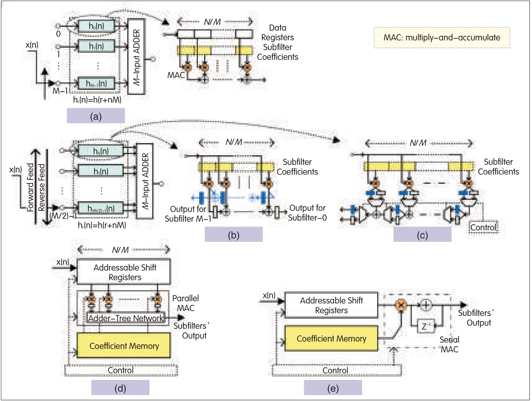
▲Figure 1.Polyphase filter structures:(a)general,(b)symmetric,(c)adder-shared symmetric,(d)serialpolyphase with parallel MAC,and(e)serialpolyphase with serial MAC.
The general M-path polyphase filter structure has M subfilters of length N/M,where N is the length of a non-partitioned lowpass filter.Each of these subfilters operates at 1/M times the input rate(Fig.1a).In the symmetric structure,the symmetry property of the coefficients in the subfilters is exploited,and this reduces the number of subfilters and commutator length to M/2.The commutator moves in both the forward and reverse feed directions(Fig.1b),and the multipliers are shared by the two subfilters[6].The adders can also be shared by using multiplexers and de-multiplexers to form an adder-shared symmetric structure(Fig.1c).In an M-path polyphase filter,only one subfilter is processed at a time,and the remaining M-1 subfilters are idle.The serial polyphase structure merges the subfilters’data registers to form a data-register bank and merges the subfilters’coefficients to form a coefficient bank.These data register and coefficient banks are addressed by a control sequence so that the data registers and coefficients of the desired subfilter can be selected to perform MAC operations.The MAC operations can be performed in parallel or in serial so that a serial polyphase structure with parallel MAC(Fig.1d)or serial MAC(Fig.1e)is formed[7].
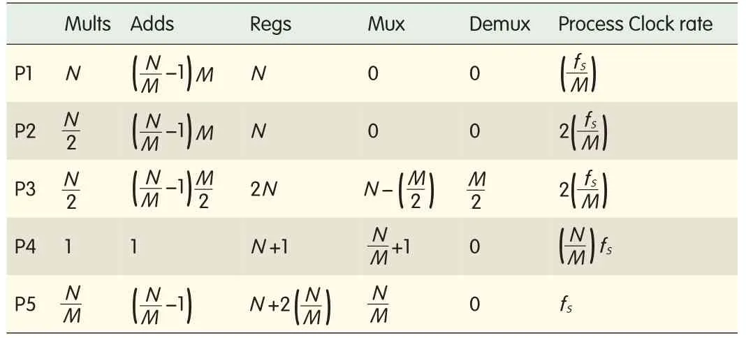
▼Table 1.Resource complexities and required process clock rates for an M-path polyphase filter with P1-P5 polyphase structures(with fs as the input rate)
Table 1 shows the resource complexity in an M-path polyphase filter(each path with N/M taps)for a general polyphase structure(P1),symmetric structure(P2),adder-shared symmetric structure(P3),and serial polyphase structure with serial MAC(P4)and parallel MAC(P5).It also shows the required operating clock rates for these structures(with fsas the input rate).There is a trade-off between complexities and processing clock rates.A serialpolyphase filter with serial MAC has the least complexity but demands a high clock rate.A serial polyphase filter with parallel MAC has a slightly higher complexity and operates at a clock rate that corresponds to the input clock rate.Among all the solutions which do not operate at a clock rate higher than the input clock rate,the P5 uses the least resources.
A non-maximally decimated polyphase filter bank processes M subfilters in a time period which is either less or greater than the M data-load’s time period.The embedded resampling in the polyphase filter banks requires architectural changes for the structures(Fig.1)to meet the output time constraint.These changes mainly apply to the structures which are sharing resources(P2,P3,P4 and P5).P1 is a fully parallel solution and is not operationally affected in non-maximally decimated modes because each subfilter is operating independently and M subfilters can be processed even for a single data input time period.However,it does require some changes in its state machine.Symmetric structures are limited to cases with an even number of polyphase partitions to make use of filter symmetry which is not the case for serialpolyphase structures.Here,we describe the mapping of P5 onto the target platform—a Xilinx Virtex-5 FPGA(xc5vsx50t-3ff1136)[8].A fixed-point analysis has been used to determine the word lengths that keep quantization errors below 60 d B(commonly required).
There are a number of design options that correspond to the level of FPGAresource exploitation.The targeted polyphase filter used for the embedded resampling cases[3]has five paths each with six taps.A straightforward mapping of the corresponding P5 structure onto an FPGA,where all the filter coefficients and the subfilters’tapped delay lines are implemented as combination logic blocks(CLBs),results in relatively high usage of slice registers and LUTs.The implementation scales linearly with the filter size.Today’s FPGAs have rich architectures with special memory resources such as distributed RAM and block RAM,high-performance computational resources such as DSP48Eslices in addition to the basic CLBs.The DSP48Eslice improves flexibility,utilization,and efficiency of applications.It also reduces overall power consumption,increases maximum frequency,and reduces setup and clock-to-out time[9].The efficient use of these dedicated resources creates a high-performance system with high operating clock rates and reduced CLB requirements.
The filter coefficient bank can be easily replaced by FPGA block RAMs to eliminate the number of CLBresources;however,the polyphase-partitioned data bank(register bank)is a bit critical because it has to shift the new data element to the respective subfilter’s tap-delay line and having access to all the taps of that subfilter at the same time.In a maximally decimated system,where the down-sampling factor is equal to the polyphase partition,a first-in first-out(FIFO)can be used as delay lines to derive the optimal architecture,as described in[9].For non-maximally decimated systems,a two-dimensionalmemory solution is required in which only the targeted subfilter can be loaded with the input data.Fig.2 shows the resource usage when mapping a 5×6 register bank(with 32-bit complex data)according to different design options available on the Virtex-5 FPGA.The 5×6 register bank based on slice registers and LUTs uses 960 slice registers and 389 LUTs.Each data register in the subfilters is replaced with a RAM-based shift register(SRL16/SRL32 mode of the slice LUTs),and the number of slice registers and LUTs usage becomes 0 and 389,respectively.This eliminates the need for slice registers,but the LUTusage remains unchanged.In Virtex-5,each CLB has 64-bit distributed RAM[8]that is bit-addressable.For a 32-bit data register,32 CLBs are collectively used as a single 32-bit register.The remaining 63 bits in each CLB are unused.Distributed memory is used so that each 64-bit memory contributes one bit to a 32-bit data register for 64 subfilters(only five are used).In this way,the memory that was previously used for only one data register of a subfilter is now used for one data register for all five subfilters.The resource usage for a 5×6 register bank based on distributed RAM becomes 192 slice registers and 192 LUTs.This eliminates the need for the decoder and multiplexers to select the desired subfilter’s data elements in the case of a shift-register-based register bank.The same concept can be applied to block RAM,which eliminates CLB usage.Three block RAMs are used for a 5×6 register bank,which corresponds to 2%utilization of block RAM resources for a Virtex-5.
To use block RAM-based register banks,an extra clock cycle is needed for each data load and shift[10]because six block RAMs(32-bit×5)are cascaded to form a 5×6 register bank,and the data shift in the subfilters requires data to be available from the preceding memory.Therefore,one clock cycle is needed to read the(previous)data elements in the cascaded memories.The next clock cycle loads the new data element to the subfilter’s data memory along with data shifting because block RAMs have synchronous read and write operations.A distributed RAM-based register bank has no extra clock cycle penalty for each data load and shift because it has asynchronous read and synchronous write operations.
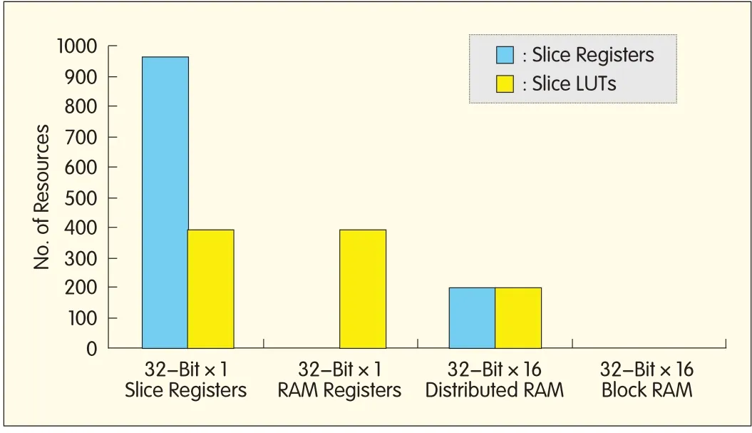
▲Figure 2.Resource usage for a 5×6 register bank by exploiting FPGAresources.
3 LPA and RA Scheduling
According to the polyphase channelizer configurations for the presented embedded resampling factors[3],five polyphase subfilters need to be processed within the time period of five,three,and six samples and within the time period of zero-packed five and 15 samples.For the resampling cases,where the number of data-loads is less than M(the number of subfilters),it is not possible to process at the input sample rate of fsin a serial polyphase structure with parallel MAC.Fig.3 shows the time domain view of the under-decimated case where 3-to-1 down-sampling is performed in a 5-path polyphase filter.The five subfilters are to be processed within the time period of three data samples.
In[10],an LPAwith block RAM-based register bank for a polyphase filter bank operating in under-decimated mode is described.This LPA runs at a higher clock rate and uses a FIFO to interface with the input data at lower rate.Fig.4 shows this architecture with an output accumulator instead of an FFTto represent the channel at baseband.In the load phase,the data elements are taken from the input FIFO and loaded into the subfilters as directed by the data pointer.In the processing phase,coefficient and data pointers with embedded shifts select the coefficient and data memory elements in order to perform MAC operations.The multipliers are based on DSP48Eslices whereas the additions are performed using a CLB-based adder tree network.
The LPAs for the five embedded resampling cases[3]are based on the architecture shown in Fig.4 according to the number of subfilters(five),number of subfilter taps(six),and corresponding data loading and filter coefficient sequences.The register and coefficient banks are based on block RAMs.Table 2 shows the operating clock rates for the designed LPAs.These clock rates meet the output time constraints of the five different cases,without overflowing the input FIFO.Cases 4 and 5 have two different load times because two different numbers of data inputs are loaded,as shown in Table 4 and Table 5 in[3].
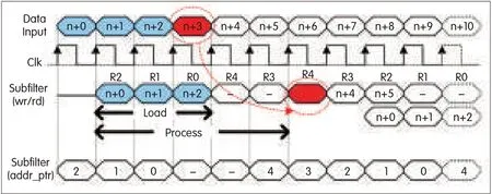
▲Figure 3.Under-decimated case where 3-to-1 down sampling is performed in a 5-path polyphase filter.The five subfilters are to be processed within the timeperiod of three data samples.
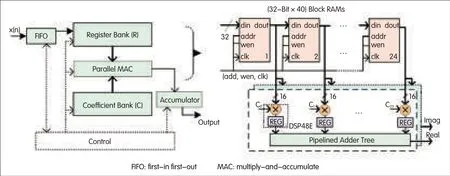
▲Figure 4.LPAwith block RAM-based register bank for a polyphase filter operating in under-decimated mode and with a clock rate higher than the input data rate.
The loading of LPA data from the input FIFO into the register bank is controlled by the FIFO empty flag,so the loading process may need to wait for the valid data sample in the FIFO.The loading time shown in Table 2 incorporates this waiting time.From Table 2,on average,approximately 60%of the loading time is used for loading the register bank.This eventually requires high operating clock rates in order to process the loaded data within the output time constraints.Although block RAMs do not require CLBs,the synchronous write and read operations require two clock cycles for loading and shifting the input data.Thus,the clock rates must be increased.On the other hand,the distributed RAM-based register bank has asynchronous read operation and only requires one clock cycle for loading and shifting.Therefore,the overall clock rate is reduced,but CLB resources are now required.

▼Table 2.Required operating clock rates for the five embedded resampling cases in a polyphase filter with block RAM-based register bank

▼Table 3.Required operating clock rates for the five embedded resampling cases in a polyphase filter with distributed RAM-based register bank
In the LPAwith distributed RAM-based register bank,the coefficient bank is based on block RAM which requires the coefficient pointer to be one clock cycle ahead of the data pointer that drives the distributed RAM-based register bank.The operating clock rates for the LPA using distributed RAM-based register bank are listed in Table 3.These clock rates meet the output time constraints of the five different cases,without overflowing the input FIFO.
From Table 2 and Table 3,it can be seen that using distributed RAM-based register banks instead of block RAM-based register banks reduces the required operating clock rates for the LPA by approximately 20%.High clock rates for LPA may limit the polyphase filter design to a lower input sample rate because the technology platform has limited ability to achieve high operating clock rates.To overcome the high clock rate demands of the LPA,we introduce the runtime architecture(RA),which runs at a maximum of double the input data rate for the five cases.At double the input data rate,it efficiently schedules the processes of M subfilters within N data load times while simultaneously loading N subfilters.It uses a distributed RAM-based register bank and also eliminates the input FIFO for bridging the input data rate with the high processing clock rate.The RA resembles the LPA(Fig.4)but has a different configuration of distributed RAM-based register bank,lacks FIFO,and has a run-time scheduling instead of a load-process scheduling.Here we present the scheduling schemes for the RA for the five embedded resampling cases[3].
Case 1:
Fig.4a[3]shows the first two loading cycles for the maximally decimated system.The timing diagram for these cycles(Fig.5)shows the scheduling of the filter operations and input data loading at the input rate.The parallel multipliers and adder tree take four clock cycles to generate the subfilters’MAC output,which are further accumulated over five MAC outputs to get the output of the polyphase filter(channel 0).
Case 2:
Fig.4b[3]shows the first two loading cycles for the under-decimated system.The timing diagram for these cycles(Fig.6)shows the scheduling of the filter operations and input data loading at double the input rate.
The first cycle of the doubled-rate(2×)clock processes the targeted(data-loaded)subfilter while the second cycle of the 2×clock processes the subfilter that is not targeted.The three input data periods have six periods of 2×clock that(for the first load cycle)schedule the processing of the non-targeted subfilters[R4,R3]by interlacing with the processing of the targeted subfilters[R2,R1,R0].The sixth 2×clock cycle is not used because a new data sample has not yet arrived.The parallel multipliers and adder tree take four cycles of 2×clock to generate the subfilters’MAC output,which is further accumulated over five MAC outputs to obtain the output of the polyphase filter.
Case 3:
Fig.4c[3]shows the first two loading cycles for the over-decimated system.The timing diagram for these cycles(Fig.7)shows the scheduling of the filter operations and input data loading at the input rate.The loading and filter processing is the same as that described in case 1,but six input data samples are loaded instead of five,and the accumulation process is modified.The R0 subfilter in the first load cycle accepts two data loads and is processed separately.Only the second processed output for the subfilter(which is loaded twice)contributes to the final accumulation.
This second processed output for R0 subfilter also has the contribution from the first loaded data sample,so the MAC outputs from n+1 to n+5 are accumulated for the final output.
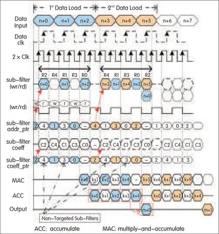
▲Figure 6.Scheduling of filter operations(at 2×clock)and input data loading for an under-decimated system(case 2).
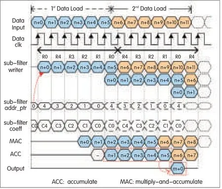
▲Figure 7.Scheduling of the filter operations(at inputclock)and inputdata loading for an over-decimated system(case3).
Case 4:
Fig.4d[3]shows the two loading cycles for the system up-sampled by two and down-sampled by five.The timing diagram for these cycles(Fig.8)shows the scheduling of the filter operations and the input data loading at double the input rate.The data loading cycle is periodic for the two states having three and two data inputs,respectively.These two states correspond to six and four cycles of 2×clock to process five subfilters.In the first state,which has three data inputs,six cycles of the 2×clock can process five subfilters.However,the second state,which has two data inputs with four 2×clock cycles,lacks a clock cycle to process the fifth subfilter.This required processing can be achieved either by using a 3×clock to provide more clock cycles or by efficiently using the non-utilized cycle of the 2×clock in the first state.In the first state,the processing of the targeted subfilters[R4,R2,R0]is interlaced with the processing of non-targeted subfilters[R3,R1].In the second state,processing of the non-targeted subfilters[R4,R2,R0]is interlaced with the processing of the targeted subfilters[R3,R1].
Case 5:
Fig.4e[3]shows the two loading cycles for the system up-sampled by two and down-sampled by 15.The timing diagram for these cycles(Fig.9)shows the scheduling of filter operations(for one loading cycle)and the input data loading at the input rate.The loading process continues for three stride lengths of the commutator,and the eight input data samples undergo filter processing.The outputs of the subfilter MACs are accumulated from outputs n+3 to n+7 because these outputs contribute to the final accumulation(which includes outputs from the twice-loaded subfilters).
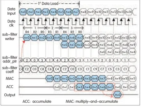
▲Figure 9.Scheduling of filter operations(at input clock)and input data loading for a system up-sampled by two and down-sampled by 15(case 5).
We have so far described the scheduling schemes for the subfilters’processes along with their data loading at the input data rate or double the input data rate.Their architectures have DSP48Eslice-based multipliers and CLB-based adder trees that limit the overall operating clock rate to approximately 200 MHz.However,the clock rate can be improved by performing MAC operations in systolic array of DSP48Eslices.To perform MAC operations in systolic arrays,the paralleldata from the data register bank needs to be time-aligned.The parallel data is fed through a set of registers that delay the data,element by element,in order to align the subfilter’s MACand final accumulation process within the systolic-array-based MAC(Fig.10).The RA with DSP48Esystolic-array-based MAC has high latency because of the pipeline and delay registers,but it increases the maximum operating clock rate to 350 MHz.The multiplexer block before the delay elements switches between the processing of the targeted subfilter and non-targeted subfilter(which is used only in cases 2 and 4).
4 Resource Usage
We have presented LPA with block RAM and distributed RAM-based register banks as well as RA(distributed RAM-based register bank)having DSP48Eslices based multipliers and CLB-based adder tree,and RA with DSP48Eslice systolic-array-based MAC.These architectures are mapped onto a Virtex-5 FPGAin the form of I/Q components.Fig.11 shows the resource usage in the FPGAfor the five embedded resampling cases.The slice registers,slice LUTs,dedicated resources,and required operating clock rates are shown for both LPAs and RAs.
In all five cases,the LPA block RAM and LPA distributed RAM(based register banks)have almost the same slice register usage,that is,397 to 407 slice registers.However,in all five cases,there is a difference in slice LUTusage between LPAblock RAM and LPA distributed RAM.The usage in LPA block RAM ranges from 406 to 431 slice LUTs,and the usage in LPA distributed RAM ranges from 447 to 502 slice LUTs.This is due to the fact that distributed RAMs(used for the data register bank)require LUTs.The variation in slice LUTusage within LPAs block RAM and LPAs distributed RAM is due to the different sets of states and controlsequences for the polyphase engines with different embedded resampling factors.The RA in all the embedded resampling cases uses almost the same number of slice registers(335-342)and almost the same number of slice LUTs(315-334).The exceptions are case 2,which has 524 slice LUTs and case 4,which has 529 slice LUTs.These two systems do not have straightforward indices for accessing their data register and filter coefficient banks.Therefore,the indices for data register and filter coefficient banks are pre-stored in LUTs instead of being generated by sets of counters.The architecture also contains the multiplexer block for switching between targeted and non-targeted subfilter processing that uses slice LUTs and slice registers.Similarly,the RA with DSP48E systolic-array-based MAC—for case 1,case 3,and case 5—have almost the same number of slice registers(318-324)and LUTs(366-381).The RA with DSP48E systolic-array-based MAC—for case 2 and case 4—use slightly more slice registers(510)and LUTs(528-563)because of the pre-stored indices for data register and filter coefficient banks,and multiplexer block.
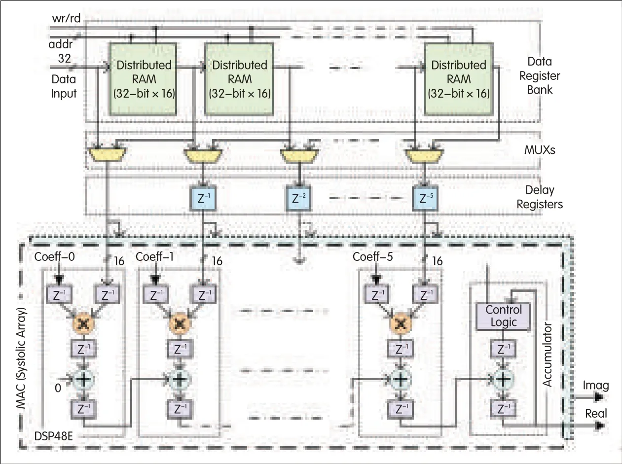
▲Figure 10.Runtime architecture with DSP48Esystolic-array based MAC.The data from the register bank is fed through a set of registers that delay the paralleldata,element by element,to align the timing of the subfilter MACand final accumulation process.
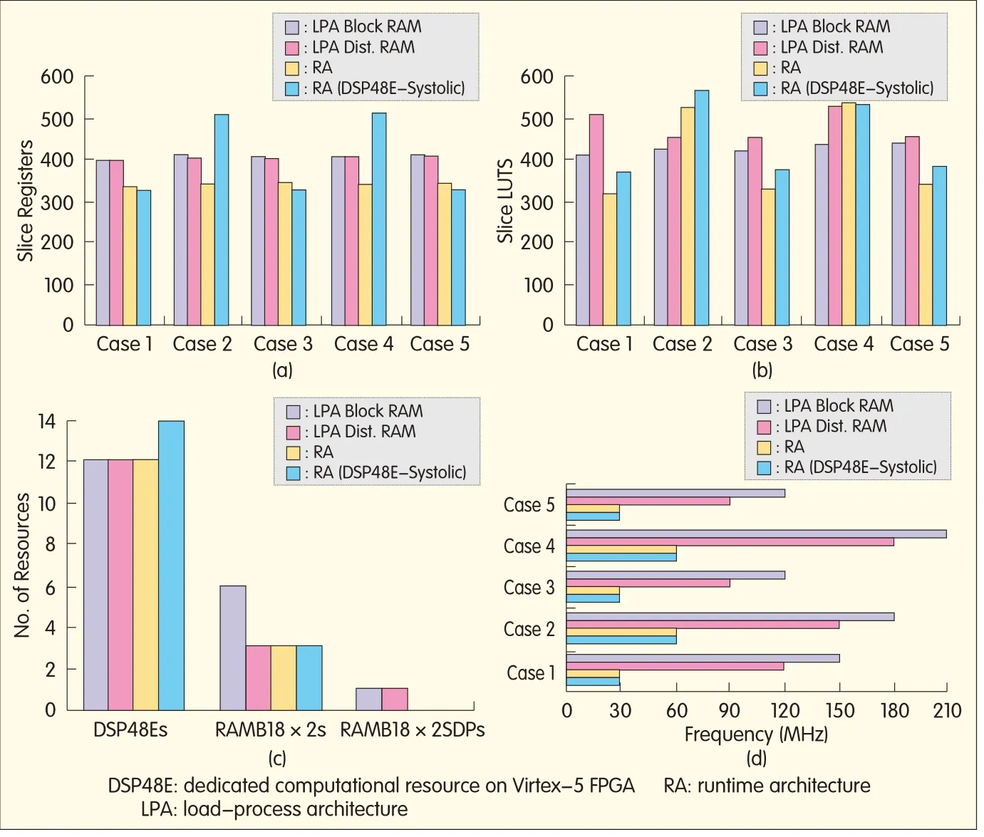
▲Figure 11.Resource usage for the five embedded resampling cases under LPAand RA:(a)slice registers,(b)slice LUTs,(c)dedicated resources,and(d)required operating clock rates.
The MAC architecture for LPA and RA has DSP48E slice-based multipliers and CLB-based adder trees.Allthe cases based on this MAC architecture uses 12 DSP48E slices.However,the RA with DSP48Esystolic-array-based MAC uses two extra DSP48Eslices for the final accumulation process.Similarly,the filter coefficient banks(which are based on block RAMs)in both LPA distributed RAM and RAs uses three dedicated RAMB18x2s[11]resources.However,the LPA block RAM uses three extra resources of RAMB18x2s for its block RAM based register bank.Furthermore,the LPAs use one RAM18x2SDPs[11]for the input FIFO(which is zero for the RAs because they do not use input FIFO).
Fig.12 shows the number of LUTs versus(operating clock)frequency for the four design solutions for the five embedded resampling cases for the polyphase filter.The RAs for case 1,case 3,and case 5 require less area and lower processing clocks than their LPA counterparts.Similarly,the RAs for case 2 and case 4 require more area but use lower processing clocks than their LPA counterparts.This larger area is due to the pre-stored indices for addressing data register and filter coefficient banks,and also due to the use of multiplexers.Thus,RA is the preferred choice for reduced operating clock rates,and also for reduced area resources with the exception of cases 2 and 4.
5 Power Analysis
Here we analyze power consumption,focusing on dynamic power(CMOStechnology is assumed)for the LPAand RAof the polyphase filter with five different resampling factors.The demand for high clock rates in the LPA is often difficult to satisfy,and the architectures are power hungry because the dynamic power is proportional to the toggle frequency[12]:

where n is the number of nodes being toggled,C is the load capacitance per node,V is the supply voltage,and f is the toggle frequency.C and V are device parameters,whereas n and f are design parameters.By keeping almost the same n and lowering f,power consumption decreases.As reduced clock operation has the same time constraint as high clock operation,energy consumption is reduced as well.
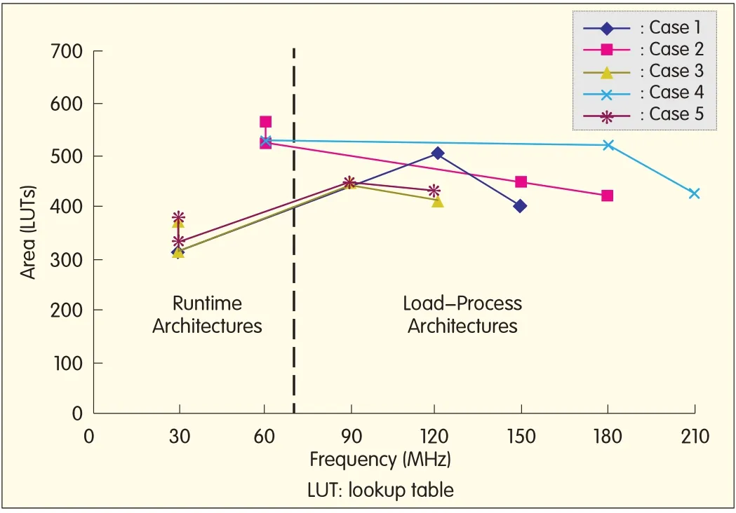
▲Figure 12.Area versus(operating clock)frequency for the four design solutions for the five embedded resampling cases.
Fig.13 shows dynamic power consumption for LPA and RA in the five embedded resampling cases.Xilinx XPA[13]tool is used.The input vector is the same for all the cases and designs,and the activity rates are calculated using ModelSim[14]post-route simulations with a run length of 500μs.The thermal settings for the power simulations are 25 degrees Celsius—an ambient temperature,and zero airflow.Fig.13 shows that the LPA with block RAM-based register bank consumes more dynamic power than LPA with distributed-RAM based register bank and also more dynamic power than RAs.The maximally decimated system(case 1)based on RAs consumes 64%less dynamic power than its LPAcounterpart when block RAM-based register banks are used,and it consumes 49%less dynamic power than its LPA counterpart when distributed RAM-based register banks are used.The under-decimated system(case 2)based on RAs consumes 48%less dynamic power than its LPA counterpart when block RAM-based register banks are used,and it consumes 27%less dynamic power than its LPA counterpart when distributed RAM-based register banks are used.The over-decimated system(case 3)based on RAs consumes 60%less dynamic power than its LPA counterpart when block RAM-based register banks are used,and it consumes 42%less dynamic power than its LPAcounterpart when distributed RAM-based register banks are used.The up-sampled by two and down-sampled by five system(case 4)based on RAs consumes 46%less dynamic power than its LPA counterpart when block RAM-based register banks are used,and it consumes 31%less dynamic power than its LPA counterpart when distributed RAM-based register banks are used.The up-sampled by two and down-sampled by 15 system(case 5)based on RAs consumes 59%less dynamic power than its LPAcounterpart when block RAM-based register banks are used,and it consumes 40%less dynamic power than its LPAcounterpart when distributed RAM-based register banks are used.Thus,RAis superior to LPAfor reducing dynamic power and clock rates.The five cases are representative for polyphase filter banks that perform embedded sample rate changes.The analysis also shows that the dynamic power for RA with DSP48E systolic-array-based MAC in cases 1,2 and 5 is between 3%to 11%higher than their RAwith DSP48Eslice-based multipliers and CLB-based adder tree.
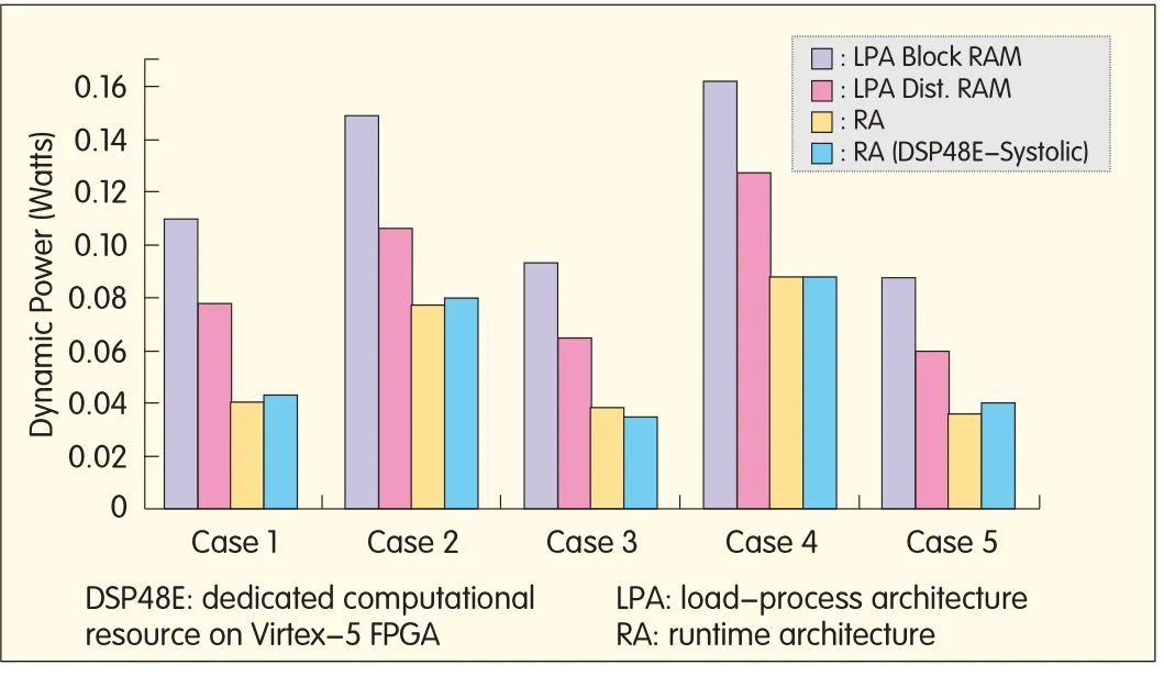
▲Figure 13.Dynamic power analysis for allfour design solutions for the five embedded resampling cases for the polyphase filter.
FPGAs provide high parallelism and reprogrammability but at the expense of additionalsignal routing resources and higher static power consumption due to transistor leakage from parasitic diodes in gate junctions[15],[16].The static current dissipates power when the device is powered-up and no logic is being clocked.The drive toward smaller transistors in FPGAis necessary for achieving higher chip density and faster dynamic speed.This,in turn,is necessary for embedding specialized DSPfunctionality blocks,but it substantially increases the current leakage.As the size of transistors in FPGA drops to 70 nm,the current leakage becomes more dominant and accounts for more than 50%of power consumption[17].The clocked(dynamic)power is added to basic static power when logic is active.Both these power contributions substantially increase as the device junction temperature increases.For the targeted Virtex-5 FPGAat 65 nm,static power consumption in all the cases of embedded resampling is around 0.660 W,significantly higher than the highest dynamic power consumption of 0.162 W.However,static power consumption is technology dependent,and only the area and clock rates can be reduced to minimize the overall power consumption in the system.
6 Conclusion
We have described the architecture and FPGA implementation of a polyphase engine that performs embedded resampling.We have analyzed the architectures for five different embedded resampling scenarios in polyphase filter banks:1)maximally decimated,2)under-decimated,3)over-decimated,and combined up-and down-sampling with 4)single and 5)multiple stride lengths of the commutator that feeds the input data into the filter bank.These scenarios are applicable to any required rational sampling rate change in a polyphase channelizer-based SDRfront-end.We have described the FPGA-based architectures for a serial polyphase structure with parallel MAC that has load-process and runtime scheduling.The LPAfirst loads the selected variable data length and then processes the subfilters that require a high clock rate.The RA,on the other hand,operates at a maximum of double the input data rate,which enables scheduling of subfilter processes along with the data loading.We have also described different design techniques for polyphase register bank mapping.A detailed analysis of area,time,and power in the two types of architectures with different resampling factors has been given.This analysis showed that RA is superior to LPAin reducing operating clock rates and dynamic power.RA is also superior in reducing area resources,except where indices are pre-stored in the LUT.Thus,RA is capable of satisfying the need for minimalarea,clock frequency,and power consumption in SDRfront-ends.From our FPGA implementation analysis,we have derived a set of valuable guidelines that can be used by system designers to create an SDRfront-end that is optimized in terms of area,time,and power consumption given certain design specifications.Future work could include a similar analysis for FPGAs from other manufacturers.This would be valuable in generalizing the suggested hardware architectures.
- ZTE Communications的其它文章
- Introduction to ZTECommunications
- AHistogram-Based Static Error Correction Technique for Flash ADCs:Implementation
- 1 Tb/s Nyquist-WDM PM-RZ-QPSKSuperchannel Transmission over 1000 km SMF-28 with MAPEqualization
- Compensating for Nonlinear Effects in Coherent-Detection Optical Transmission Systems
- The Key Technology in Optical OFDM-PON
- Design of a Silicon-Based High-Speed Plasmonic Modulator

