Magnetic proximity effect in the two-dimensional ε-Fe2O3/NbSe2 heterojunction
Bingyu Che(車冰玉), Guojing Hu(胡國(guó)靜), Chao Zhu(朱超), Hui Guo(郭輝),Senhao Lv(呂森浩), Xuanye Liu(劉軒冶), Kang Wu(吳康), Zhen Zhao(趙振),Lulu Pan(潘祿祿), Ke Zhu(祝軻), Qi Qi(齊琦), Yechao Han(韓燁超), Xiao Lin(林曉),Zi’an Li(李子安), Chengmin Shen(申承民), Lihong Bao(鮑麗宏), Zheng Liu(劉政),?,Jiadong Zhou(周家東), Haitao Yang(楊海濤),?, and Hong-Jun Gao(高鴻鈞)
1Beijing National Center for Condensed Matter Physics and Institute of Physics,Chinese Academy of Sciences,Beijing 100190,China
2School of Physical Sciences,University of Chinese Academy of Sciences,Beijing 100190,China
3School of Materials Science and Engineering,Nanyang Technological University,Singapore
4School of Physical Science and Technology,Guangxi University,Guangxi 530004,China
5School of Physics,Beijing Institute of Technology,Beijing 100081,China
Keywords: two-dimensional heterojunctions, magnetic proximity effect, non-layered magnetic nanosheet,spin–orbit interaction
1.Introduction
The exchange interaction in two-dimensional (2D)magnetic heterostructures has become an intriguing research direction due to the potential of breaking the timereversal symmetry of the originally degenerate band structures.Currently, various 2D materials have been integrated with magnetic materials, such as topological insulators,[1,2]semiconductors[3–6]and superconductors.[7]Among them,2D magnet/superconductor heterostructures are especially interesting because both systems are closely associated with the alignment of charge spin.Intuitively, superconductivity and ferromagnetism are incompatible.However, curious phenomena arise in magnet–superconductor heterojunctions, including unconventional superconductivity, topological superconductivity, and the modulation of magnetic alignment by Ising superconductivity.[7–11]Therefore, magnet/superconductor junctions offer a great platform to study the fundamental interaction between superconductivity and magnetism.Moreover, they produce significant opportunities to develop spintronics and superconducting spintronic devices.[9]
Intrinsic 2D vdW magnets have been found in Cr,Fe,V,and Mn based materials.[12]Some of the most famous ones such as CrI3,Cr2Ge2Te6,and Fe3GeTe2have weak ferromagnetic properties.[13–16]Without gate voltage modulation, the Curie temperatures (TC) of these magnetic 2D vdW materials are far below room temperature,typically,45 K for monolayer CrI3,[13,14]30 K for bilayer Cr2Ge2Te6,[15]and 130 K for monolayer Fe3GeTe2.[16]Such lowTCresults in the impossible application in the room-temperature device.Although theTCof Fe5GeTe2reaches 320 K,[17,18]magnetic 2D vdW materials reported at present are unstable in air, which hinders the exploration of their application.In contrast, nonlayered ferrimagnetic iron oxides can maintain magnetic properties up to room temperature and are stable in the ambient environment.[19]However,the study of magnetic proximity in 2Dε-Fe2O3-based devices is still at an embryonic stage.
In this paper, we developed a space-confined chemical vapor deposition (CVD) strategy to synthesize ultrathinε-Fe2O3nanosheets with thicknesses down to 3 nm.Ultrathinε-Fe2O3nanosheets have room-temperature ferrimagnetic properties and excellent air-stability.ε-Fe2O3/NbSe2heterojunctions have been constructed by a standard transfer and stacking technique to explore magnetic proximity on superconductivity of NbSe2multilayers.The result shows that the subtle proximity effect of theε-Fe2O3nanosheet can modulate the spin–orbit interaction(SOI)of the NbSe2multilayer with negligible influence on its superconducting critical parameters.Our work provides a potential platform to study proximity effects in 2D heterojunctions based on ultrathin non-layered materials.
2.Experimental details
2.1.Growth of ε-Fe2O3 nanosheets
A space-confined CVD strategy was used to synthesizeε-Fe2O3nanosheets.Theε-Fe2O3nanosheets were grown on the fluorophlogopite mica(Changchun Taiyuan Fluorophlogopite Co., China) substrate.A mixture of anhydrous ferrous chloride (FeCl2) and KCl powder with a mass ratio of about 10:1 was used as the precursor.A small amount of the precursor was put directly between two pieces of freshly cleaved mica (10 mm×10 mm in size).Before heating, the furnace was vacuumed and purged by pure argon to remove the residual oxygen and moisture.Then the furnace was heated to 640?C in 15 min and held at that temperature for 2 min before cooling down naturally to room temperature, with 100 sccm Ar and 1.5 sccm O2flowing through the furnace during the whole process.ε-Fe2O3nanosheets were grown on both pieces of mica substrates.
2.2.Sample characterization
Raman spectra were obtained by HORIBA LabRAM HR Evolution.X-ray photoelectron spectroscopy(XPS)tests were conducted in an ultrahigh vacuum system (VG ESCALAB-5) equipped with XPS.The thicknesses and the magnetic force microscopy(MFM)image ofε-Fe2O3nanosheets were obtained by Oxford Cypher S atomic force microscope.The HAADF imaging was carried out on JEOL ARM-200F(S)TEM equipped with CEOS CESCOR Cs probe corrector,using a 200 kV acceleration voltage.The convergence semiangle was set to 27–33 mrad and the collection semi-angle was 60–280 mrad for the image acquisition.Magnetization measurements were carried out by using a vibrating sample magnetometer (MPMS 3, Quantum Design).Both electrical resistance and voltage dependence of current(V–I)data were collected on a Quantum Design physical properties measurement system(PPMS).
3.Results and discussion
As shown in Fig.1(a),ε-Fe2O3has a non-symmetric orthorhombic structure, where Fe ions occupying four inequivalent sites are labeled as Fe(1),Fe(2),Fe(3),and Fe(4).[20–22]They are the centers of either an oxygen octahedron or a tetrahedron.The room-temperature ferrimagnetism ofε-Fe2O3mainly comes from Fe(3) and Fe(4), whose magnetic moments are anti-collinear with different magnitudes, while the magnetic moments of Fe(1) and Fe(2) compensate for each other.[21]ε-Fe2O3is a rare phase in the iron oxide family,which only exists in the nanoparticle form, not in the bulk form.It was hard to obtain pureε-Fe2O3single crystals because the synthetic routes involved phase transition.[22]However, some CVD methods have recently been introduced to synthesize air-stableε-Fe2O3nanosheets with thickness above 4 nm.[23–25]Here we developed a space-confined CVD technique to synthesize large non-layeredε-Fe2O3nanosheets with thinner thicknesses than the reported ones (as described in Section 2).The thinnest thickness of our as-grown hexagonalε-Fe2O3nanosheets is down to 3 nm(Figs.1(b)and 1(c)).The XPS spectrum across an area of 2×0.2 mm2confirms that all Fe ions in the nanosheets are Fe3+, with no trace of Fe2+(Fig.1(d)).[26,27]As shown in Fig.1(e), the Raman spectrum ofε-Fe2O3nanosheets has four unique Raman peaks between 100 cm-1and 200 cm-1as hallmarks to verify theε-Fe2O3phase,which do not exist inγ-Fe2O3orα-Fe2O3phase.[23,28]The Raman mapping result of a typical nanosheet indicates the pureε-Fe2O3phase in the whole sample(Fig.1(f)).
Scanning transmission electron microscopy (STEM)characterization was carried out to get a clearer understanding of the atomic arrangement and quality of the as-synthesizedε-Fe2O3nanosheets.In the large-area ADF(annular dark field)image of theε-Fe2O3nanosheet along thec-axis (Fig.2(a)),there are no lattice defects across the whole area,indicating the high crystalline quality of the nanosheet.The Fourier transform of the large-area ADF image in Fig.2(b)shows only one set of spots,which is consistent with the simulated diffraction pattern along thec-axis of theε-Fe2O3crystal(Fig.2(c)).In the zoomed image of the large-area ADF image,a perfect honeycomb lattice composited of spots with different brightness is observed(Fig.2(d)).The brightness of the spots corresponds to different compositions of the atom columns beneath the sample surface.As the oxygen atoms have less contribution to the ADF signals than the iron atoms, the columns with more iron atoms are much brighter than those with fewer iron atoms.The experimental image matches well with the simulated ADF image(Fig.2(e))and the crystalline structure(Fig.2(f)).The intensity of the experimental signals also agrees with the simulated data in Fig.2(g), which demonstrates the high quality of theε-Fe2O3nanosheets.
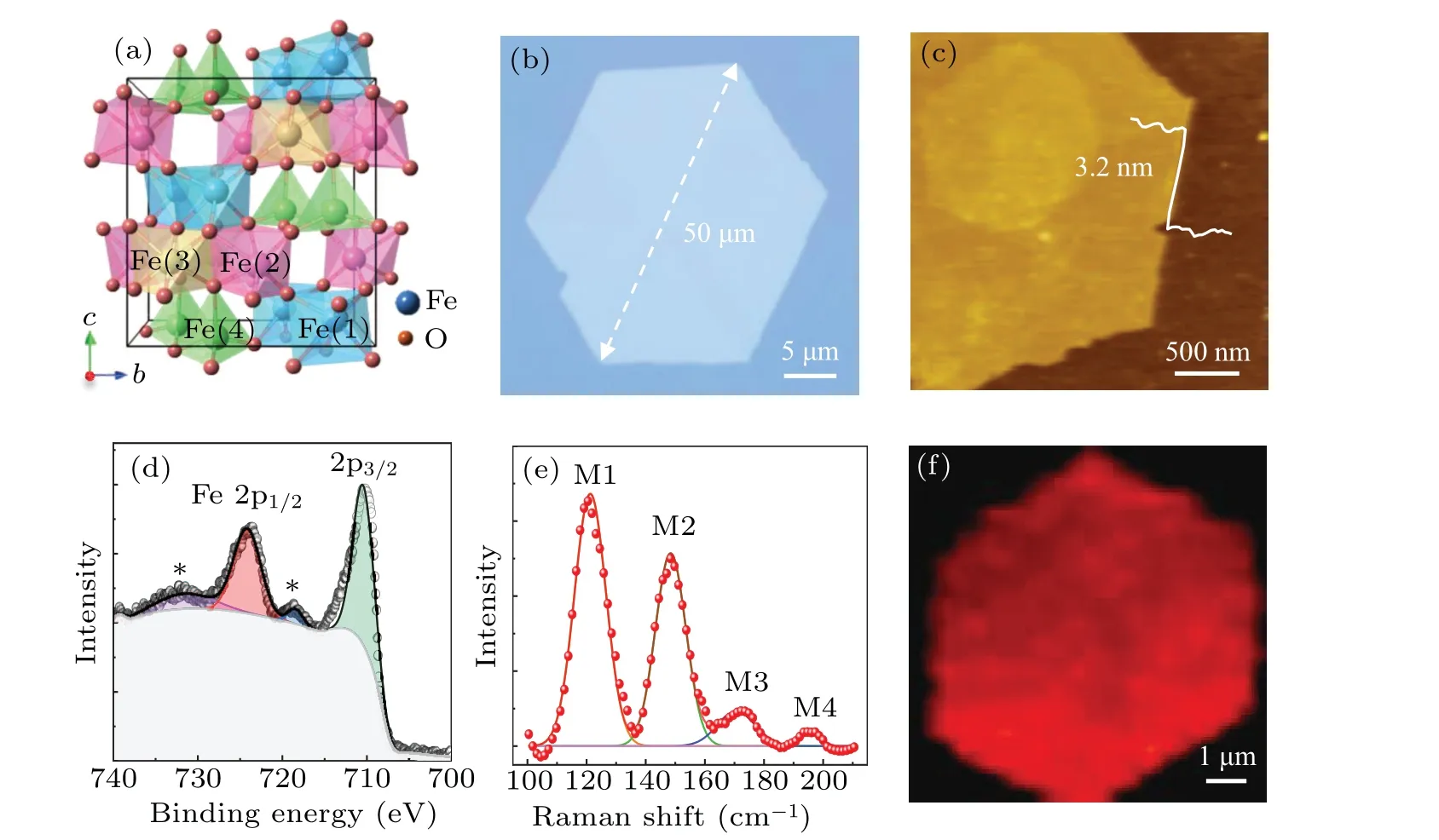
Fig.1.(a) Crystalline structure of ε-Fe2O3.(b), (c) Optical and AFM images of a typical ε-Fe2O3 nanosheet, showing the lateral size and thickness.(d) XPS of ε-Fe2O3 nanosheets on the mica substrate.The circles and the lines are the experimental and fitting data.(e) Raman spectrum of the ε-Fe2O3 nanosheet.The red dots and the solid lines are the experimental and fitting data.(f)Raman mapping of the ε-Fe2O3 nanosheet,showing the uniform chemical distribution.The sum range is between 100 cm-1 and 200 cm-1.
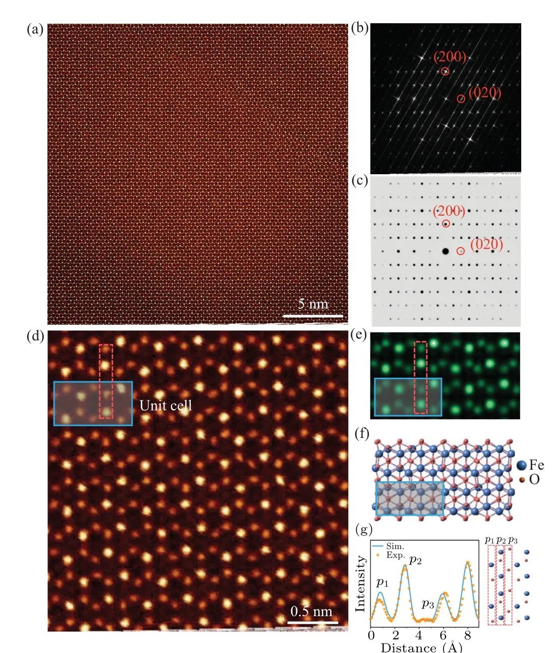
Fig.2.STEM analysis of the ε-Fe2O3 nanosheet.(a)Large-area ADF-STEM image of the ε-Fe2O3 nanosheet.(b) The Fourier transition pattern of (a).(c)The simulated diffraction pattern of ε-Fe2O3.(d),(e)Zoomed ADF-STEM image of the ε-Fe2O3 nanosheet and its corresponding simulated image.The blue rectangular highlights one unit cell.(f) The crystalline structure along the c-axis of ε-Fe2O3.The highlighted unit cell in the blue rectangular perfectly matches those in(d)and(e).(g)The peak intensity of the atom columns marked by the red rectangular in(d)and(e).The yellow dots are the experimental data,which agrees well with the simulated light blue line.
To study the magnetic properties ofε-Fe2O3nanosheets,temperature-dependent (M–T) and field-dependent (M–H)magnetization measurements were employed.In theM–Tcurves(Fig.3(a)),theε-Fe2O3nanosheets exhibit a slight decrease of magnetization until 350 K in the field cool procedure(FC).There are also two kinks in the curve measured in the FC procedure, which is similar to that of their nanoparticle counterparts.[22,29,30]The two kinks correspond to two magnetic transitions,the one around 160 K involves the direction change of the magnetic easy axis, and the other around 133 K is related to a decrease of the coercive field.In theM–Hcurves under different temperatures(Fig.3(b)),theε-Fe2O3nanosheets exhibit a well-defined hysteresis loop at 300 K,indicating ferrimagnetic properties at room temperature.[22]The magnetic force microscopy(MFM)image on a singleε-Fe2O3nanosheet shows a uniform phase contrast,indicating a single domain structure at room temperature(Fig.3(c)).
The high-quality ultrathinε-Fe2O3nanosheets with room-temperature ferrimagnetic properties can be a good candidate for exploring the magnetic proximity effect.Therefore,we constructedε-Fe2O3/NbSe2heterojunctions to get further insight into magnetic proximity on superconductivity.The ultrathinε-Fe2O3nanosheet has an energy gap of about 1.9 eV,consistent with its nanoparticle counterpart.[19]Althoughε-Fe2O3is a non-layered material, the as-synthesizedε-Fe2O3nanosheets and the mica substrate are weakly bonded.[23]Therefore,the nanosheets can be easily transferred by a standard water-assisted method.NbSe2is a van der Waals layered type-II superconductor,[31–33]which can be exfoliated into few layers to form a magnet/superconductor heterojunction withε-Fe2O3nanosheets.As the resistance of the NbSe2multilayer is much smaller than that of theε-Fe2O3nanosheet, the current in this device can be considered to flow mainly through the NbSe2layer.To realize a precise comparison of the superconducting properties in theε-Fe2O3/NbSe2heterojunction and the NbSe2multilayer, we designed a two-channel device structure on one NbSe2multilayer.As shown in Fig.3(d), a NbSe2multilayer with uniform thickness was transferred on a group of pre-deposited parallel bottom electrodes, and then theε-Fe2O3nanosheet with a thickness of about 10 nm was stacked only on the right four electrodes to construct theε-Fe2O3/NbSe2heterojunction.The electrical transport properties of the NbSe2multilayer and theε-Fe2O3/NbSe2heterojunction were measured in two separate channels.TheR–Tcurves of the NbSe2multilayer and theε-Fe2O3/NbSe2heterojunction show that their critical temperatures (Tc) are 6.39 K and 6.38 K (Fig.3(e)).The almost unchangedTcin the heterojunction is because the in-plane magnetic moments ofε-Fe2O3nanosheets generate little stray field penetrating the NbSe2multilayer.[34]The resistance dependence of outof-plane fields (R–H⊥curves) was also measured at different temperatures.The temperature-dependent upper critical fields (H⊥c2–T) were extracted and fitted with the linear 2D Ginzburg–Landau model[35]
whereΦ0is the quantum flux andξGLis the in-plane superconducting coherent length.The in-plane orbit-limiting pair breaking fields of the NbSe2multilayer and theε-Fe2O3/NbSe2heterojunction are determined to be 5.68 T and 5.54 T from the extrapolation ofH⊥c2at 0 K.And the superconducting coherent lengths are calculated as 7.62 nm and 7.71 nm for the NbSe2multilayer and the heterojunction, respectively.
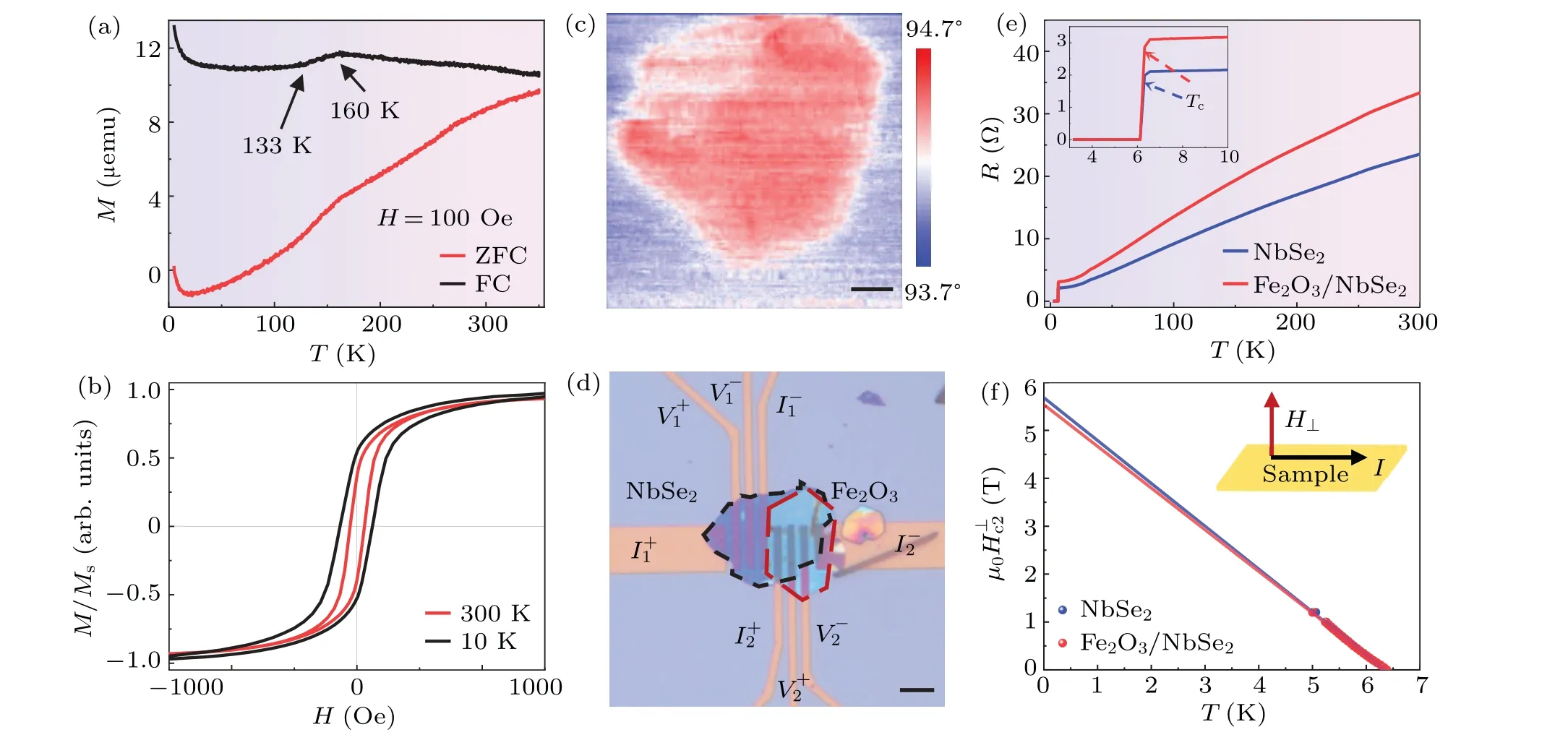
Fig.3.Magnetic properties of ε-Fe2O3 nanosheets and the superconductivity of the ε-Fe2O3/NbSe2 heterojunction.(a), (b) Temperaturedependent and field-dependent curves of ε-Fe2O3 nanosheets.(c) The MFM image of a typical ε-Fe2O3 nanosheet, indicating the uniform magnetic state.(d) The optical image of the ε-Fe2O3/NbSe2 heterojunction device.(e) The R–T curves of the NbSe2 multilayer and the ε-Fe2O3/NbSe2 heterojunction.The inset is the R–T curves from 3 K to 10 K.Tc is defined as the temperature where the resistance reaches 90%of the normal resistance at 7 K.(f)The linear fittings for the out-of-plane upper critical magnetic fields(H⊥c2–T)of the NbSe2 multilayer and the ε-Fe2O3/NbSe2 heterojunction. Hc2 is defined as the field where the resistance reaches 90%of the normal resistance.The scale bars in(c)and(d)are 0.5μm and 5μm.
The resistance dependence of the in-plane field (R–H‖curves) at different temperatures was also studied.Small humps are observed near the upper critical fields of the superconducting transition of theε-Fe2O3/NbSe2heterojunction at high magnetic fields, while such a feature does not exist in the NbSe2multilayer (Figs.4(a) and 4(b)).The humps are probably induced by the flow of Josephson vortices.The applied in-plane fields will induce interlayer Josephson vortices in the NbSe2multilayer, which penetrate theε-Fe2O3nanosheet.Since the vortices are weakly pinned in theε-Fe2O3nanosheet, when a current perpendicular to the field flows through them,the vortices can be de-pinned and driven by the Lorentz force.The collective movement of the Josephson vortices leads to large energy dissipation and results in a limited magnetoresistance.[36,37]TheH‖c2–Tcurves were also plotted and fitted with in-plane 2D Ginzburg–Landau model[35]
wheredSCis the effective thickness of the superconductor.The superconducting effective thicknesses can be obtained to be 8.53 nm and 8.94 nm for the NbSe2multilayer and theε-Fe2O3/NbSe2heterojunction.Thus,the obtainedTc,Hc2,ξGLanddSCin the NbSe2multilayer andε-Fe2O3/NbSe2heterojunction are concluded nearly the same.
BesidesTcandHc2, the critical supercurrent (Ic) is another important parameter for a superconductor.Therefore,V–Icurves for both the NbSe2multilayer and theε-Fe2O3/NbSe2heterojunction were also measured to study the magnetic proximity effect on superconducting properties.Although theIcis nearly the same at about 0.45 mA for both the NbSe2multilayer and theε-Fe2O3/NbSe2heterojunction, the transition from the superconducting state to normal state (?I) is different (Fig.4(d)).The ?Ifor the heterojunction is much larger than that for the NbSe2multilayer, which might result from the interaction between the magnetic moment of theε-Fe2O3nanosheet and the magnetic flux generated by the current in the NbSe2multilayer.[38]TheV–Imeasurements were also carried out under different out-of-plane magnetic fields.The field-dependent critical currentsI+c(I-c) at a positive (negative) bias were extracted from theV–Icurves.A field-induced nonreciprocal charge transport for the NbSe2multilayer was observed (Fig.4(e)), which is significantly suppressed in theε-Fe2O3/NbSe2heterojunction (Fig.4(f)).The nonreciprocal critical current under positive and negative bias originates from the valley-Zeeman spin–orbit interaction(SOI)of NbSe2.[39,40]In NbSe2few layers,the electron spin is locked with valleys in the out-of-plane direction.[41]When an out-of-plane field is applied, the degeneracy of valleys with opposite momenta is broken by the Zeeman effect,which will possibly induce asymmetric pinning potentials in the NbSe2multilayer.[42]And the collective flow of the vortices in the NbSe2multilayer driven by the external charge current among these asymmetric pinning potentials will cause nonreciprocal transport behavior.[40,43]This phenomenon is suppressed under high fields,similar to the previously reported results.[40,44–47]In the heterojunction, theε-Fe2O3nanosheet on top of the NbSe2multilayer might generate a complex pinning effect that competes with the asymmetric pinning potentials generated by the valley-Zeeman SOI in NbSe2to interference the vortex flow, and therefore suppresses the nonreciprocal transport behavior.The results indicate that the strong SOI exists at the interface between the nonlayeredε-Fe2O3nanosheet and the NbSe2multilayer, and prove that theε-Fe2O3nanosheets are smooth and clean enough to construct 2D heterojunctions.
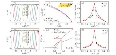
Fig.4.Electrical transport properties of the NbSe2 multilayer and the ε-Fe2O3/NbSe2 heterojunction.(a),(b)The R–H curves of the NbSe2 and the ε-Fe2O3/NbSe2 heterojunction regions.The red arrow in(b)indicates the hump which appears near H‖c2 at high fields.(c)The fitting curves for in-plane H‖c2–T of the NbSe2 multilayer and the ε-Fe2O3/NbSe2 heterojunction.(d)The V–I curves of the NbSe2 multilayer and the ε-Fe2O3/NbSe2 heterojunction at 2 K.?I is the current range of superconducting transition.(e),(f)The out-of-plane magnetic field-dependent positive and negative Ic extracted from the V–I curves of the NbSe2 multilayer and the ε-Fe2O3/NbSe2 heterojunction.
4.Conclusion
We successfully synthesized high-qualityε-Fe2O3nanosheets by a space-confined CVD method and verified its high crystalline quality by STEM characterization.The magnetic measurements show that theε-Fe2O3nanosheets remain ferrimagnetic up to 350 K.An ultrathinε-Fe2O3nanosheet was used to construct theε-Fe2O3/NbSe2heterojunction to study the magnetic proximity effect on superconductivity of NbSe2multilayer.The electrical transport results demonstrate that theTc,Hc2andIcin the NbSe2multilayer andε-Fe2O3/NbSe2heterojunction are nearly the same,indicating that theε-Fe2O3nanosheet has a minor influence on the superconductivity of the NbSe2multilayer.However,the proximity effect of theε-Fe2O3nanosheet shows an obvious modulation effect on the interfacial SOI, which suppresses the nonreciprocal transport of the NbSe2multilayer.This work shows that non-layered ferrimagneticε-Fe2O3nanosheets can form 2D heterojunctions with other 2D vdW materials to modulate their properties by proximity effect, which enables theε-Fe2O3nanosheets and further non-layered 2D magnets with stronger perpendicular anisotropy[48]to be potential building blocks for spintronics and superconducting spintronic devices.
Acknowledgements
We thank Gangqin Liu for the helpful discussions.The work is supported by the National Key Research and Development Program of China(Grant No.2022YFA1204104),the National Natural Science Foundation of China (Grant No.61888102), the Chinese Academy of Sciences (Grant Nos.ZDBS-SSW-WHC001 and XDB33030100).
- Chinese Physics B的其它文章
- Quantum synchronization with correlated baths
- Preparing highly entangled states of nanodiamond rotation and NV center spin
- Epidemic threshold influenced by non-pharmaceutical interventions in residential university environments
- Dynamical behavior of memristor-coupled heterogeneous discrete neural networks with synaptic crosstalk
- Dynamics and synchronization in a memristor-coupled discrete heterogeneous neuron network considering noise
- Spatial search weighting information contained in cell velocity distribution

