Intrinsic electronic structure and nodeless superconducting gap of YBa2Cu3O7-δ observed by spatially-resolved laser-based angle resolved photoemission spectroscopy
Shuaishuai Li(李帥帥), Taimin Miao(苗泰民), Chaohui Yin(殷超輝), Yinghao Li(李穎昊),Hongtao Yan(閆宏濤), Yiwen Chen(陳逸雯), Bo Liang(梁波), Hao Chen(陳浩),Wenpei Zhu(朱文培), Shenjin Zhang(張申金), Zhimin Wang(王志敏), Fengfeng Zhang(張豐豐),Feng Yang(楊峰), Qinjun Peng(彭欽軍), Chengtian Lin(林成天), Hanqing Mao(毛寒青),5,Guodong Liu(劉國(guó)東),5, Zuyan Xu(許祖彥), Lin Zhao(趙林),5, and X J Zhou(周興江),5,?
1National Laboratory for Superconductivity,Beijing National Laboratory for Condensed Matter Physics,Institute of Physics,Chinese Academy of Sciences,Beijing 100190,China
2University of Chinese Academy of Sciences,Beijing 100049,China
3Technical Institute of Physics and Chemistry,Chinese Academy of Sciences,Beijing 100190,China
4Max Planck Institute for Solid State Research,Heisenbergstrasse 1,D-70569 Stuttgart,Germany
5Songshan Lake Materials Laboratory,Dongguan 523808,China
Keywords: YBCO,angle resolved photoemission spectroscopy,electronic structure,superconducting gap
1.Introduction
The superconductivity mechanism of the high temperature cuprate superconductors remains one of the most prominent issues in condensed matter physics.[1]The detection of intrinsic electronic structure and the determination of the superconducting gap symmetry are essential in understanding the unusual normal state properties and the superconductivity mechanism of the cuprate superconductors.Angle resolved photoemission spectroscopy (ARPES) has played a key role in studying the cuprate superconductors.[2–5]However, most of the ARPES measurements are carried out on the Bi-based superconductors, particularly Bi2Sr2CaCu2O8(Bi2212), because it is easy to get a smooth surface of the cleaved sample and measure the intrinsic electronic structure of the bulk material.Much fewer ARPES measurements have been performed on YBa2Cu3O7-δ(Y123), another prototypical cuprate superconductor with aTcabove the liquid nitrogen temperature.[6–25]Because the cleaved surface of Y123 is polar which causes charge redistribution and surface selfdoping, it is difficult to probe the intrinsic electronic structure of the bulk Y123.[6,8,10,13,15,17]In particular, the Fermi surface-dependent and momentum-dependent superconducting gap has not been clearly determined in Y123.[20,21,23]The measurement of the intrinsic bulk electronic structure and superconducting gap in Y123 is important in establishing a general picture in understanding high temperature superconductivity in cuprate superconductors.
In the present paper,we report our observations of the intrinsic electronic structure and superconducting gap of Y123.By performing spatially-resolved laser-based ARPES,we successfully find the cleaved region where the CuO2planes are not self-doped and measure the electronic structure and superconducting gap intrinsic to the bulk Y123.The Fermi surfacedependent and momentum-dependent superconducting gap is clearly determined and a nodeless d-wave gap is observed in Y123.
2.Methods
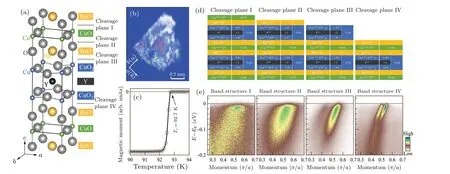
ARPES measurements were carried out using our labbased laser ARPES systems equipped with the 6.994 eV vacuum-ultra-violet (VUV) laser and a DA30L hemispherical electron energy analyzer.[26,27]The laser spot was focused to~15 μm on the sample.The energy resolution was set at 1 meV and the angular resolution was~0.3?, corresponding to a momentum resolution of~0.004 ?A-1.High quality single crystals of YBa2Cu3O7-δwere grown by the self flux method.[28]The samples were post-annealed at 494?C under oxygen pressure of~1 atmospheres for 7 days.The obtained samples were optimally doped with aTcof 92.7 K and a transition width of~0.3 K(Fig.1(c)).The measured samples were twinned.All the samples were cleavedin situat a low temperature and measured in vacuum with a base pressure better than 5×10-11Torr at 17 K.The Fermi level was referenced by measuring on a clean polycrystalline gold that was electrically connected to the samples.
3.Results and discussion
Through real-space point-by-point ARPES scanning measurements(Fig.S1 in supplementary materials),we found mainly four kinds of band structures on the Y123 cleavage surface, as shown in Fig.1(e).The band structure I has a broad band with a diffuse distribution of intensity in momentum space.It exhibits a clear energy gap at the Fermi level.The band structure II also has a broad band but without energy gap opening at the Fermi level.The band structure III shows two bands that are well separated in the momentum space.Both bands do not show energy gap opening at the Fermi level.The band structure IV shows two sharp bands which are close in the momentum space.Both bands show energy gap opening at the Fermi level.Figure 1(b)shows the spatial distribution of the band structures III and IV on the cleaved sample surface.These two regions occupy only a small fraction(<5%)of the surface area while the majority of the surface is occupied by the band structures I and II.
Figure 1(a)shows the crystal structure of Y123.It is usually considered that the cleaving occurs between the BaO layer and CuO chain layer,giving rise to two cleavage planes I and II.[25,29,30]But only two kinds of cleavage planes can not account for the four kinds of band structures we have observed.Two more cleavage planes have to be considered that occur between the BaO layer and the CuO2layer,marked as cleavage planes III and IV in Fig.1(a).In Fig.1(d),we show these four kinds of cleavage planes and analyze the charge distribution among different layers.It turns out that all these four cleavage planes are polar and, according to the polar catastrophe model,[31]there is charge redistribution on the top layer.As a result,the CuO2planes are self-doped with the doping level increase from the original 0.16 to 0.33 in the cleavage planes II and III.This makes the top CuO2planes heavily overdoped and become nonsuperconducting.But the CuO2planes keep their doping level 0.16 in the cleavage planes I and IV.This makes it possible to retain its intrinsic electronic structure and keep it at the optimal doping level.

By considering the charge distribution in different cleavage planes in Fig.1(d) and the gap opening in the four kinds of band structures in Fig.1(e), and also considering the big(small)chance of cleavage for the cleavage planes I and II(III and IV)and the large(small)occupation of the band structures I and II(III and IV),we can make a good correspondence between the four cleavage planes and the observed four kinds of band structures.In particular,the band structure IV originates from the cleavage plane IV where the top CuO2planes keep their original doping level 0.16.Both bands are sharp with clear gap opening.Therefore,the electronic structures are intrinsic to the bulk Y123.It is the first time that this kind of band structure has been observed in Y123 because its occupation area is rather small in the cleaved sample surface.We will focus on this band structure in the rest of the paper.
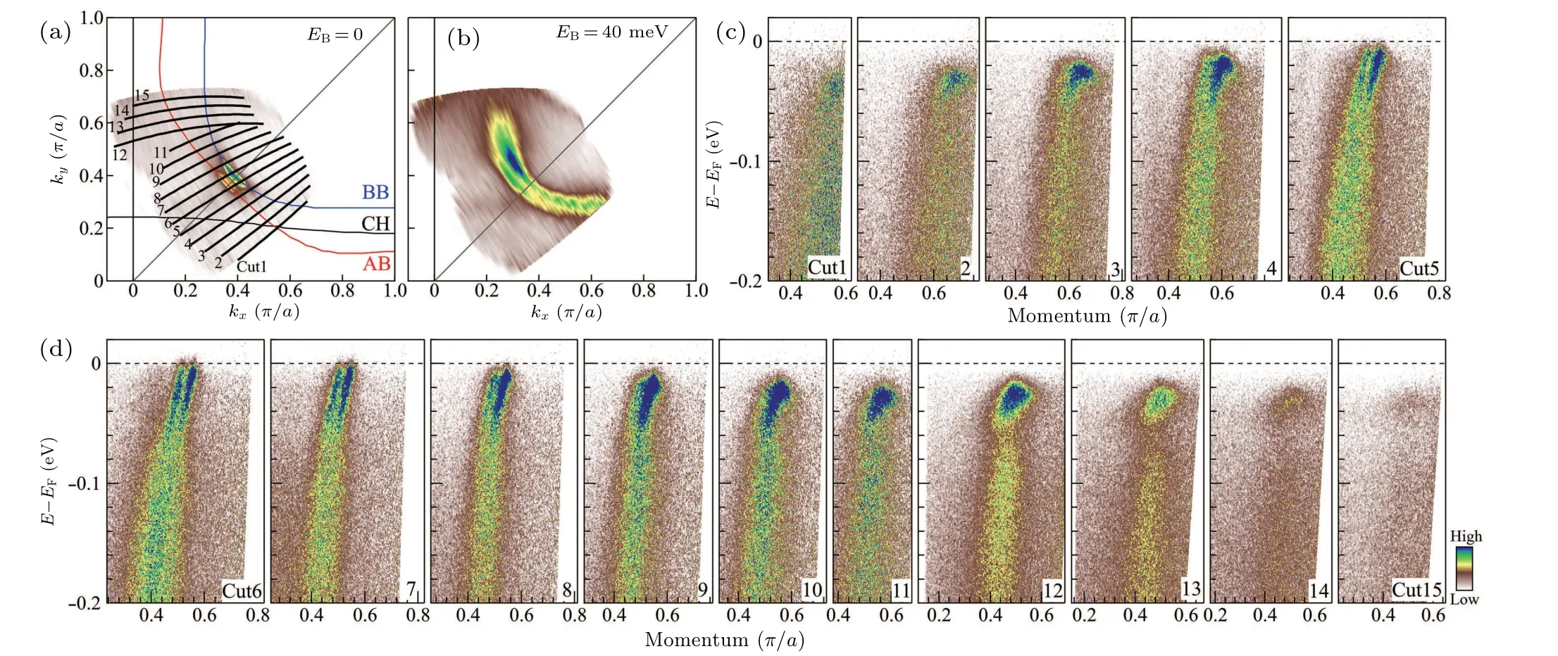
Figure 2 shows the Fermi surface and band structures of Y123 measured at 17 K from the red region in Fig.1(b).During the measurements,we overcome two technical issues.The first is the space charge effect caused by the small laser spot;we reduced the laser intensity to alleviate the space charge effect.The second is the light-induced modification effect; the measured area is modified by the light illumination over a period of time.To reduce the effect, we limited our acquisition time to finish the measurement on one region before the obvious sample modification occurs.These two issues put a strong limit on the data statistics.
Two bands are clearly observed that correspond to the bonding band (BB) and the antibonding band (AB) in Y123.The bonding band can be observed over a wide momentum space from the nodal to the antinodal regions.It becomes weaker when the momentum cut moves to the antinodal region.The gap opening at the Fermi level can be clearly observed on the bonding band which gets larger with the momentum cut moving from the nodal to the antinodal regions.On the other hand, the antibonding band is clearly observed only around the nodal region; it becomes invisible when the momentum cut moves away from the nodal region.By considering the Fermi surface mapping in Fig.2(a)and the corresponding band structures in Fig.2(c), and also referring to the Fermi surface measured from the previous ARPES measurements,[23]we arrived at the Fermi surface of the optimally-doped Y123 as plotted in Fig.2(a) which consists of the bonding Fermi surface(BB),the antibonding Fermi surface(AB),and the chain Fermi surface(CH).
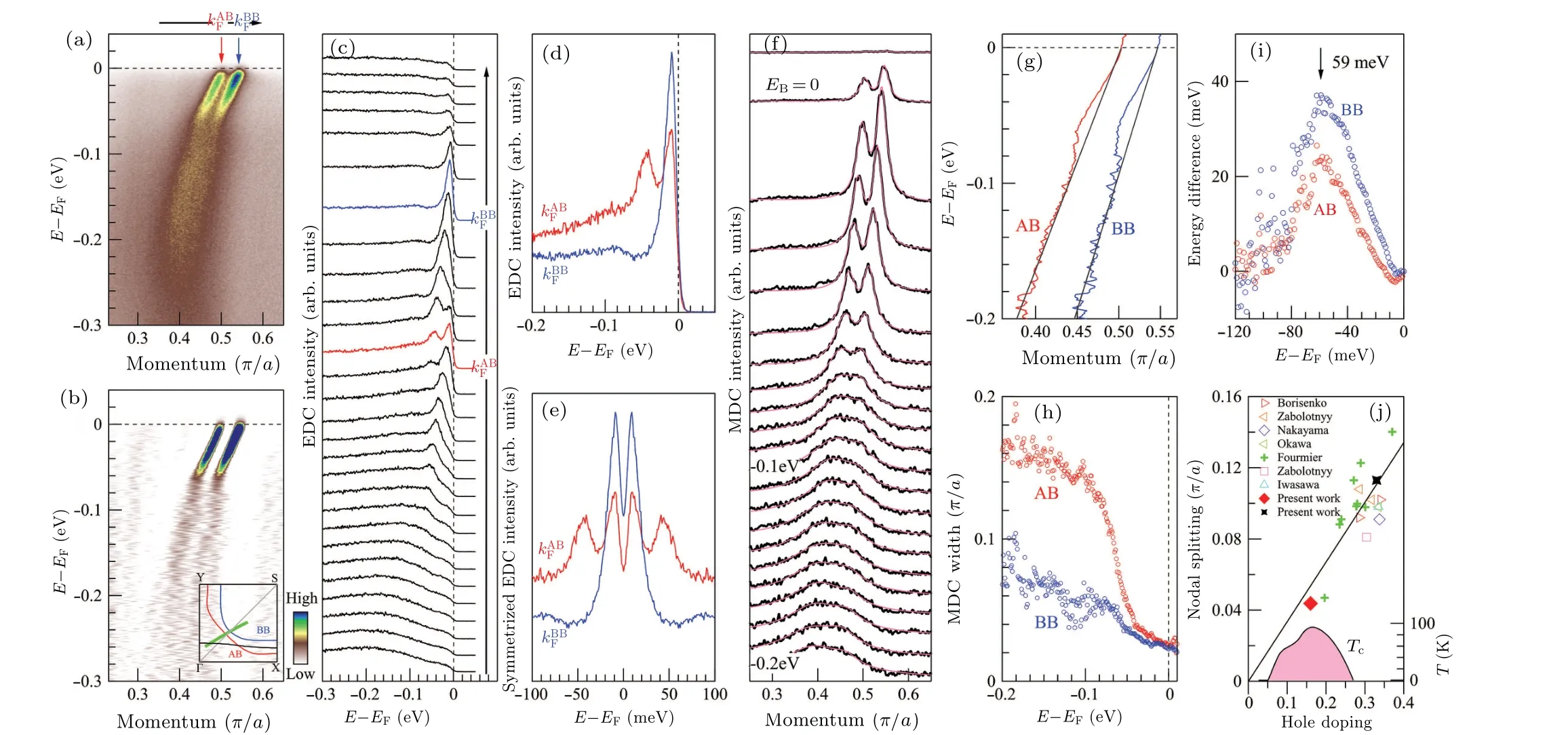
Figure 3 focuses on the band structure of Y123 along the nodal direction.Two sharp bands are clearly observed in Fig.3(a) which correspond to bilayer split bonding and antibonding bands.These two bands become more clearly observed in the second derivative image in Fig.3(b).The corresponding photoemission spectra(energy distribution curves,EDCs) show sharp superconducting coherence peaks as seen in Fig.3(c).The EDCs at the two Fermi momenta are plotted in Fig.3(d) and their corresponding symmetrized EDCs are shown in Fig.3(e).Clear superconducting gap opening is observed on the two Fermi surfaces along the nodal direction.
Figure 3(f)shows momentum distribution curves(MDCs)at different energies obtained from Fig.3(a).These MDCs can be well fitted by using two Lorentzians.The fitted dispersions and the MDC widths are plotted in Figs.3(g) and 3(h), respectively.The AB and BB bands exhibit clear kink in their dispersions (Fig.3(g)), accompanied by the drop in their MDC width (Fig.3(h)).To reveal the kink structure more clearly, in Fig.3(i), we plot the energy difference between the measured dispersions and straight lines as shown in Fig.3(g).Well-defined peaks at~59 meV are observed in Fig.3(i)which corresponds to the kink position in the dispersions in Fig.3(g).The dispersion kink can be attributed to the electron-mode coupling.We note that,since the measured region keeps the original doping level,our measured kink structure is obviously stronger than those previously measured in self-doped Y123.[16,22]


In Fig.3(j),we summarize the nodal bilayer splitting observed by the ARPES measurements on Y123 with different doping levels.[16,17,20,21,23–25]Here the doping level has been corrected from their nominal values by considering the polar catastrophe model and the self-doping effect.The nodal bilayer splitting increases with the increasing doping level.This relation can be used to check the real doping level of the measured region by measuring the nodal bilayer splitting.The nodal bilayer splitting in our measurement is the smallest.This further confirms that our measured region has the optimal doping level 0.16 and our measured electronic structures are intrinsic to the optimally-doped bulk Y123.
Now we come to the determination of the superconducting gap in Y123.Figure 4(a) shows EDCs along the bonding Fermi surface.The corresponding symmetrized EDCs are plotted in Fig.4(b).These symmetrized EDCs can be fitted by the Norman formula[32]to extract the superconducting gap.The obtained superconducting gap at different locations of the BB Fermi surface is plotted in Fig.4(f).Likewise, Fig.4(c)shows EDCs along the antibonding Fermi surface and their corresponding symmetrized EDCs are presented in Fig.4(d).These symmetrized EDCs are also fitted by the Norman formula and the obtained superconducting gap for the AB Fermi surface is also plotted in Fig.4(f).
As seen from Fig.4(f), the optimally-doped Y123 exhibits a superconducting gap (~7 meV) even along the nodal direction.This is different from the other cuprate superconductors where the nodal superconducting gap is basically zero.[33]The presence of the s component in the superconducting gap of Y123 was also reported in the tunneling experiment.[34]The optimally-doped Y123 is different from other cuprate superconductors in that it has an orthorhombic crystal structure due to the presence of the CuO chain along thebdirection.Whether the small anisotropy betweenaandb(~2%) can cause such an obvious nodal gap needs further investigations.
For a standard d-wave form,there is a zero gap along the nodal direction(θ=45?)(Fig.4(g)).When there is an s component mixed in the d-wave form, there are two possibilities.One is the d+s form which still has gap node but the node position shifts away fromθ=45?(Fig.4(h)).When there are two domains present like in Y123,they will produce two kinds of gap form as shown in Fig.4(h).The other is the d+is form where there is no longer gap node present(Fig.4(i)).Our measured superconducting gap in Fig.4(f)appears not consistent with the d+s form because no gap node is observed.It is consistent with the d+is form and the measured superconducting gap can be well fitted by the d+is form,as shown in Fig.4(f).
4.Summary
In summary,we have carried out spatially-resolved laserbased ARPES measurements on the optimally-doped Y123 superconductor.We find the region from the cleaved surface that represents the bulk electronic properties.The intrinsic Fermi surface and band structures of Y123 are obtained.Nodeless superconducting gap is observed which is consistent with the d+is gap form.
Acknowledgements
Project supported by the National Natural Science Foundation of China (Grant Nos.11888101 and 11974404),the National Key Research and Development Program of China(Grant Nos.2021YFA1401800 and 2018YFA0704200),the Strategic Priority Research Program (B) of the Chinese Academy of Sciences (Grant Nos.XDB25000000 and XDB33000000),the Youth Innovation Promotion Association of CAS(Grant No.Y2021006),Innovation Program for Quantum Science and Technology (Grant No.2021ZD0301800)and the Synergetic Extreme Condition User Facility(SECUF).
- Chinese Physics B的其它文章
- The application of quantum coherence as a resource
- Special breathing structures induced by bright solitons collision in a binary dipolar Bose–Einstein condensates
- Effect of short-term plasticity on working memory
- Directional-to-random transition of cell cluster migration
- Effect of mono-/divalent metal ions on the conductivity characteristics of DNA solutions transferring through a microfluidic channel
- Off-diagonal approach to the exact solution of quantum integrable systems

