Precisely controlling the twist angle of epitaxial MoS2/graphene heterostructure by AFM tip manipulation
Jiahao Yuan(袁嘉浩) Mengzhou Liao(廖夢舟)Zhiheng Huang(黃智恒) Jinpeng Tian(田金朋)Yanbang Chu(褚衍邦) Luojun Du(杜羅軍) Wei Yang(楊威) Dongxia Shi(時東霞)Rong Yang(楊蓉) and Guangyu Zhang(張廣宇)
1Beijing National Laboratory for Condensed Matter Physics and Institute of Physics,Chinese Academy of Sciences,Beijing 100190,China
2School of Physical Sciences,University of Chinese Academy of Sciences,Beijing 100049,China
3College of Semiconductors(College of Integrated Circuits),Hunan University,Changsha 410082,China
4Songshan Lake Materials Laboratory,Dongguan 523808,China
5Department of Control Engineering,Faculty of Electrical Engineering,Czech Technical University in Prague,Czech Republic
Keywords: AFM tip manipulation,MoS2/graphene heterostructure,twist angle,moir′e superlattice
1. Introduction
Because of the weak van der Waals (vdW) interactions,two-dimensional(2D)materials can be stacked together without the constraints of lattice matching[1]and thus possess a fascinating degree of freedom — interlayer twist angle.[2–5]Realizing precise control of the interlayer twist angle is of the utmost importance to engineer the twistronics and a variety of novel physical properties, such as unconventional superconductivity,[6]moir′e excitons,[7]nonlinear optics[8]and magnetism.[9]For the most commonly used ‘tear and stack’techniques,[6]although the interlayer twist angle can be controlled precisely in principle,the inevitable inhomogeneity of twist angle, interface bubble and the inability to manipulate it lead to poor reproducibility and hinder the further development of twistronics.[10–12]On the other hand,for the epitaxial growth method,2D moir′e superlattices with perfect interfaces can be obtained,but their interlayer twist angle is usually in the most stable thermodynamic configuration.[13,14]Remarkably,the recent advance shows that benefiting from the ultra-low interfacial friction,[15,16]the twist angle of 2D moir′e materials can be manipulated by an atomic force microscope(AFM)tip,[17–21]endowing the possibility to continuously tune the twist angle with high accuracy.
In this work, we demonstrated the control of the twist angle of epitaxial MoS2/graphene heterostructure with an ultra-high accuracy via AFM tip manipulation. High-quality MoS2/graphene 2D heterostructures were epitaxially synthesized by chemical vapor deposition (CVD) to achieve clean and flat interfaces without bubbles. An AFM tip was used to control the interlayer twist angle. By precise manipulation of the AFM tip at the nanometer scale, we achieved accurate control of the interface twist angle with precision below 0.1?.Conductive AFM (C-AFM), Raman and photoluminescence(PL) spectroscopy were performed to show the effect of the twist angle on moir′e pattern wavelength, phonons and excitons. The implementation of this technique will be very useful for the fabrication and study of 2D moir′e material systems.
2. Experimental details
2.1. Epitaxial growth of samples
The MoS2/graphene 2D heterostructure was grown by a home-made three-temperature-zone CVD system.[14]S (Alfa Aesar, 99.5%, 6–10 g) and MoO3(Alfa Aesar, 99.9995%,20 mg) as precursors were placed in zone-I and zone-II.Graphite was mechanically exfoliated on a 300 nm SiO2/Si substrate in zone-III. During growth, Ar/O2(gas flow rate,325/1 sccm)was used as the carrier gas and the pressure was maintained at 1.00 Torr. The temperatures in the three zones were 120?C,565?C and 960?C,respectively,and the growth time was about 25 min.
2.2. Spectroscopic characterizations
A Horiba Jobin Yvon LabRAM HR-Evolution Raman system was used to carry out Raman and PL characterizations.The wavelength of the excitation laser was 532 nm.
2.3. AFM/C-AFM imaging and friction measurements
An Asylum Research Cypher S system was used to perform AFM imaging and friction measurements. AFM imaging and friction measurements used an AC200-TS-R3 tip of which the vertical and lateral sensitivity was 630.70 nN/V and 6632.43 nN/V.[15,22]C-AFM imaging used an ASYELEC-01-R2 tip with Ti/Ir coating and the 901.730 holder. All the measurements were performed in ambient conditions (20–25?C and 10%–20%R.H.).
3. Results and discussion
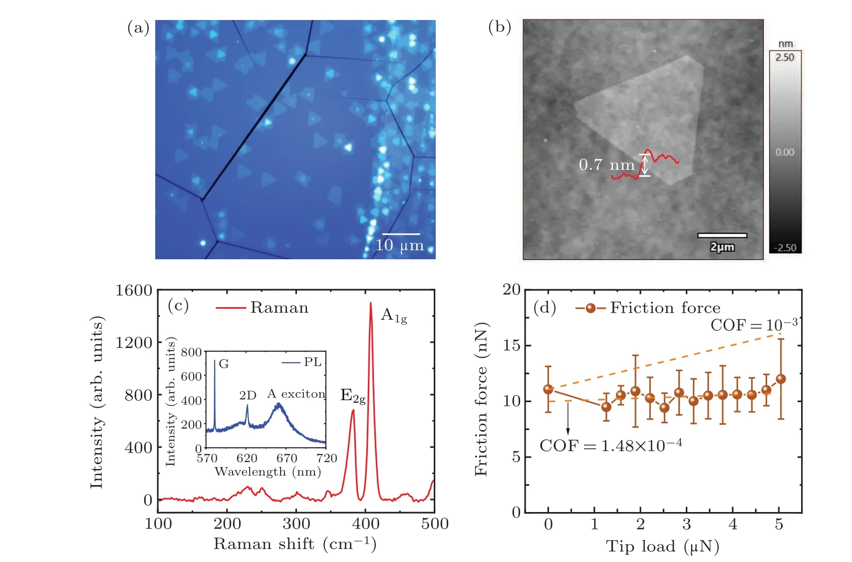
As shown in Fig. 1(a), the epitaxial MoS2domains are about micron size and have both 0?and 60?orientations.AFM image of Fig.1(b)shows that the thickness of MoS2domains is around 0.7 nm, indicating the monolayer nature. The interface of the sample is flat and clean. The Raman spectrum of Fig. 1(c) shows an E2gpeak at 383.0 cm?1and an A1gpeak at 407.8 cm?1. The PL spectrum has a strong A exciton peak at 661.4 nm. We can also see the G peak of graphene at 580.8 nm and the 2D peak at 621.8 nm, and the G/2D peak height ratio indicates that the graphene was only fewlayered.[23,24]Since MoS2and graphene have a large lattice mismatch of 28.4%, the interface forms an incommensurate configuration, achieving structural superlubricity with ultralow friction.[15,16,25]The friction properties of the heterogeneous interface were characterized by the lateral force mode of AFM.By pushing the boundary of the MoS2flake or dragging the sample to move back and forth with an AFM tip,the magnitude of the friction force at the sample interface can be measured by observing the abrupt change of the lateral force signal.[15]Figure 1(d)shows the variation of the friction force at the interface between a MoS2flake and graphene under different normal forces applied by the tip. It can be seen that the friction force at the interface does not vary significantly with the change of the tip load,and the average friction force is 10.56 nN, which is maintained at an extremely low level.The coefficient of friction (COF) at the interface is also only 1.48×10?4, much less than 10?3, which confirms the structural superlubricity property of the heterogeneous interface of MoS2/graphene.

Fig.1. Characterizations of MoS2/graphene heterostructures. (a)Optical image of as-grown MoS2 domains on few-layer graphene. (b)AFM image of a MoS2 flake on a graphene substrate. (c) Raman and PL spectra of MoS2/graphene heterostructures. (d) Friction force between MoS2 and graphene as a function of tip load.
The superlubricity of MoS2/graphene interface allows us to manipulate the twist angle with an AFM tip. First,the tapping mode of AFM should be used to obtain the topography of the sample. Then the AFM tip must be engaged in contact mode so that the tip can be in contact with the upper surface of graphene. We can manipulate the AFM tip to follow any path that we specify on the sample surface from one point to another point,either straight or curved. When the tip touches the edge of the MoS2flake, due to the ultra-low friction at the MoS2/graphene interface, the force exerted by the tip can drive the MoS2to move on the surface. However,as this system reaches the lowest energy state at 0?/60?,[14]a simple push by an AFM tip can only achieve a translational motion of the MoS2domains on graphene,rather than a rotation. Therefore,we need to add an extra external force to form a combined torque to control the twist angle of the heterogeneous structure. Figure 2(a)is a schematic illustration of the twist angle modulation method. In our experiments, we used the MoS2steps pinned at graphene boundaries and graphene wrinkles as the fulcrum for the rotation of MoS2and applied a pushing force with an AFM tip on the outside to generate a combined torque.By controlling the direction and route of the tip’s movement,different twist angles can be achieved. Moreover,the accuracy of the angle control enabled by this AFM tip manipulation method can be very high. As shown in Fig. 2(b),point O, where the MoS2flake contacts the boundary edge,was set as the rotation axis. We used the AFM tip to push point A,the farthest point away from point O in this domain,and made it rotate along the normal direction of OA at 15 nm(Figs. 2(c)–2(d)). Since the length of OA was 8.97 μm, this MoS2flake rotated clockwise by 0.096?. By high-resolution scanning and finely controlling the path of the AFM tip, the accuracy of the twist angle modulation can reach an order of magnitude of 0.1?and even lower. Figures 2(e)–2(h) are the AFM images of the system achieving different twist angles under the manipulation of the AFM tip. We chose 9.0?,36.0?and 61.5?as our targets and the results were in agreement with what we expected. It can be seen that by this approach, it is possible to achieve rotational control of the 2D heterostructure at any certain angles we want. Apart from MoS2/graphene,AFM tip manipulation can also be applied to other vdW heterostructures and homostructures,e.g.,bilayer graphene,to realize the high-precision controlling of the twist angle if the interface is clean and incommensurate.

Fig. 2. Twist angle control of MoS2/graphene heterostructure. (a) Schematic diagram of the method to control the twist angle between MoS2 and graphene by an AFM tip. (b)–(d)A demonstration of precise control of interlayer twist angle below 0.1?. (e)–(h)AFM images of MoS2/graphene heterostructure at different twist angles we want.
After achieving the precise control of the MoS2/graphene twist angle by an AFM tip, we used C-AFM to characterize the heterostructure with different twist angles from 0?to 60?.The applied bias was 1.5 V with a current limit of±20 nA and noise of 1.5 pA.A 110-M? resistor was connected in series into the circuit to prevent current overload. Figure 3(a)shows the C-AFM image of the 0?MoS2/graphene sample.After a fast Fourier transform (FFT), two sets of hexagonal spots occurred(inset of Fig.3(a)),corresponding to the moir′e superlattice (red) and MoS2lattice (blue), respectively. Figures 3(b)–3(e) show the C-AFM images of MoS2/graphene moir′e patterns after the FFT filter at different twist angles,and it can be seen that the period of the moir′e superlattice varies significantly at different angles, indicating the significant effect of the twist angle. The clear and regular moir′e patterns confirm that the twist angle distribution in the heterostructure is uniform, and the interface is not contaminated. The moir′e wavelengthλcan be theoretically calculated by

whereδis the lattice mismatch between MoS2and graphene,ais the graphene lattice constant, andθis the relative twist angle.[26]Figure 3(f) shows the theoretical and measured MoS2/graphene moir′e wavelength and MoS2lattice constants from 0?to 60?. For the moir′e superlattice,the period first decreases and then increases gradually. It reaches the maximum at 0?and 60?, and the minimum around 30?, which is consistent well with the theoretical curves. Note that the lattice constant of MoS2does not change with the twist angle.
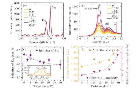
We also conducted spectroscopic characterizations of the MoS2/graphene at different twist angles.Figures 4(a)and 4(b)show the Raman and PL spectra of the heterostructure modulated by the interlayer twist angle from 0?to 30?. The PL spectra are normalized by the G peak of graphene. It can be seen that the peak shape of E2gRaman mode, as well as the PL intensity and emission energy of the monolayer MoS2, are strongly dependent on the twist angle. The peak of MoS2E2gmode splits and broadens(inset of Fig.4(c))under in-plane strain resulted by moir′e superlattice. As shown in Fig.4(c), the splitting of E2gpeak decreases as the interlayer twist angle increases from 0?to 30?, revealing that the strain in MoS2is gradually getting smaller.[27,28]Also, as shown in Fig. 4(d), when the twist angle increases from 0?to 30?,the A exciton PL peak position is gradually blue-shifted, and its energy increases by 11.6 meV, which is either attributed to misorientation-induced lattice strain.[29]PL intensity of A exciton increases by a factor of 4.64 from 0?to 30?due to the transition of the MoS2band gap from indirect at 0?to direct at 30?.[30]These results are consistent with the previous work,[18]indicating that this twist angle control method can produce clean 2D moir′e materials with highly precise and continuously controlled twist angle.

Fig. 4. Spectroscopic characterizations of the MoS2/graphene heterostructure. Raman (a) and PL (b) of MoS2/graphene at different twist angles. The splitting of E2g mode peak(c),energy and relative PL intensity of A exciton(d)associated with the interlayer twist angle.
4. Conclusion and perspectives
In summary,we demonstrated a method to precisely control the interlayer twist angle of epitaxial MoS2/graphene heterostructure by an AFM tip. This technique is convenient and suitable for other 2D moir′e homo- and heterostructures with incommensurate interfaces. The accuracy of twist angle control enabled by this method can reach the order of 0.1?and even below. C-AFM, Raman and PL spectra were conducted to characterize the moir′e patterns, phonons and excitons of MoS2/graphene at different angles. Our work provides guidance for the fabrication of 2D twist-angle-dependent incommensurate homo- and heterostructures with clean interfaces and high angular accuracy and uniformity.
Acknowledgement
Project supported by the Natioanl Natural Science Foundation of China(Grant Nos. 62122084,12074412,61888102,and 11834017).
- Chinese Physics B的其它文章
- Direct measurement of two-qubit phononic entangled states via optomechanical interactions
- Inertial focusing and rotating characteristics of elliptical and rectangular particle pairs in channel flow
- Achieving ultracold Bose–Fermi mixture of 87Rb and 40K with dual dark magnetic-optical-trap
- New experimental measurement of natSe(n,γ)cross section between 1 eV to 1 keV at the CSNS Back-n facility
- Oscillation properties of matter–wave bright solitons in harmonic potentials
- Synchronously scrambled diffuse image encryption method based on a new cosine chaotic map

