Charge transfer modification of inverted planar perovskite solar cells by NiOx/Sr:NiOx bilayer hole transport layer
Qiaopeng Cui(崔翹鵬) Liang Zhao(趙亮) Xuewen Sun(孫學(xué)文) Qiannan Yao(姚倩楠)Sheng Huang(黃勝) Lei Zhu(朱磊) Yulong Zhao(趙宇龍)Jian Song(宋健) and Yinghuai Qiang(強穎懷)
1The Jiangsu Province Engineering Laboratory of High Efficient Energy Storage Technology and Equipments,School of Materials Science and Physics,China University of Mining and Technology,Xuzhou 221116,China
2Advanced Analysis&Computation Center,China University of Mining and Technology,Xuzhou 221116,China
Keywords: perovskite solar cells,nickel oxide,Sr doping,bilayer hole transport layer
1. Introduction
Solar cells have attracted a great deal of attention,and the most glamorous star is organic-inorganic hybrid perovskite solar cells (PSCs) now. In recent years, researchers have concentrated on PSCs because of their rapid growth in power conversion efficiency (PCE).[1-5]So far, the PCE of PSCs has reached 25.2%,[6]their performance has almost caught up with currently commercialized silicon solar cells. Hybrid perovskite materials have many advantages, such as adjustable band gap, high absorption coefficient, long carrier life, and high carrier mobility.[7-10]Therefore, PSCs have potential to become the flagship of commercial solar power generation after silicon solar cells.[11]However,interface energy loss of different functional layers and alignment mismatch of energy levels still hinder performance enhancement of PSCs. Many scientists have made efforts in this regard.[12]Chenet al.reached a PCE of 19.35% by employing a NiOxhole transport layer(HTL) with Cs.[13]Chenet al.suppressed the interfacial recombination by facile alkali chloride interface modification of the NiOxHTL and obtained a device with PCE of 21%.[14]Zhuet al.used a larger alkylammonium interface layer to reduce the energy loss between the transport layer and the perovskite, and successfully achieved a inverted PSCs efficiency record of 22.3%.[15]Therefore, improving layer-to-layer interface is essential to promote the charge transfer process and to reduce carrier recombination so as to further improve the PCE.[16]
HTLs are designed to block electrons,enhance hole transport and prevent quenching caused by direct contact between the perovskite layer and conductive substrate in inverted PSCs.There are many HTLs based on polymers or small molecules,such as Spiro-OMeTAD, PEDOT:PSS, PTAA, and P3HT.[17]However, due to the natural instability of organic materials and relatively low work function, researchers are also actively studying inorganic hole transport materials. Inorganic p-type semiconductor materials, such as NiO, CuI, CuSCN,and graphene oxide are also taken as HTLs in inverted planar PSCs.[18-21]Among them, NiOxhas suitable work function,natural stability,and great energy level matching,which is widely used in the devices.[22,23]
However,NiO has a low intrinsic conductivity,which will cause holes to accumulate at the NiOx/perovskite interface and to reduce hole extraction ability,so as to reduce the open circuit voltage (Voc) and efficiency of devices.[24]Researchers are actively looking for strategies to improve the optical and electrical properties of NiOxthin film. Doping can effectively improve conductivity of NiOxfilms and adjust energy band position to well match with the energy levels. Dopants,such as Sr,Cu,Li,and Co[20,25-27]have been used to enhance charge transfer performance in NiOxHTLs. However, doping not only greatly increases concentration of free carriers,but also brings lattice distortion and introduces new impurity levels, which will enlarge the possibility of carrier recombination. Therefore, doping is not always conducive to hole extraction at the interface of NiOxand perovskite. Film surface modification[28-31]or various advanced film deposition methods[32-36]can be used to relieve charge recombination at charge transfer layer(CTL)/perovskite interface.
Our group previously proposed an ingenious strategy both to enhance the hole transport ability and to suppress charge recombination at CTL/perovsktie interfaces with a pp+homojunction based on Cu doped NiOxand Li doped NiOx.[37,38]We found that other element doping such as Sr can also significantly increase the carrier concentration of NiOxfilms. In this work, we further construct a NiOx/Sr:NiOxbilayer HTL to study its influence on interface carrier transport. We prepared an inverted planar PSC with a structure of FTO/Sr:NiOx/NiOx/perovskite/PCBM/BCP/Ag,showing an enhanced hole extraction ability and energy level matching because of the NiOx/Sr:NiOxbilayer HTL. In this device,Sr-doped NiOxthin film has no direct contact with the perovskite layer. As a result, we obtain an improved PCE of 18.44% and a fill factor of 0.80 based on the bialyer HTL,which is much higher than that using Sr:NiOx(16.89%) or NiOx(15.69%).
2. Experiment
2.1. Preparation of the HTL
FTO glass(Nippon Sheet Glass)was first cut into a size of 19 mm×19 mm. The glasses was put in a glass washing rack,and washed by deionized water with dishwashing detergent,deionized water,ethanol,isopropanol,and ethanol in sequence,under ultrasonic for half an hour.Next,a precursor solution of nickel oxide was prepared,0.727 g Ni(NO3)2·6H2O was dissolved in 5 mL of ethylene glycol solution, and then 0.15 g ethylenediamine was added. For Sr doped NiOx, additional 0.04233 g Sr(NO3)2(Sr/Ni ratio in the precursor solution is 8%) was added. In order to eliminate the influence of film thickness, we used the same two-step spin coating method to prepare HTLs with three structures,including NiOx,Sr:NiOx,and NiOx/Sr:NiOx. The first layer was deposited by spin-coating under 5000 rpm for 30 s,after heating at 120°C for 10 min,the second layer was deposited by the same procedure. Finally,the film was annealed at 400°C for 1 h.
2.2. Fabrication of solar cell
A ternary cation mixed perovskite film using MA(methylammonium ion, CH3NH+3), FA (formamidine ion, HN=CHNH+3) and Cs was prepared as the active layer. We took 0.0224 g MABr, 0.1719 g FAI, 0.5071 g PbI2, and 0.0734 g PbBr2and dissolved them in a mixed solvent (1 mL) with a volume ratio of DMSO and DMF of 1:4. After two hours of thorough mixing, 84 μL of CsI (1.5 mol/L, DMSO as solvent) was added. The final formula ratio of perovskite is Cs0.1(MA0.12FA0.88)0.9Pb(I0.95Br0.05)3.Then 60 μL of filtered perovskite precursor solution was dropped on the prepared HTL film, spinning at 1000 rpm for 10 s, and then sped to 4000 rpm. After 8 s, 200 μL of ethyl acetate was quickly dropped. The obtained perovskite film was then heated at 70°C for 3 min, and 100°C for 10 min. Next, 45 μL of PCBM(25 mg/mL,chlorobenzene as solvent)was spin-coated at 3000 rmp for 30 s to prepare the electron transport layer.Subsequently,45 μL of BCP(0.5 mg/mL,ethanol as solvent)was deposited on PCBM at 3000 rpm for 30 s. Finally,a vacuum thermal evaporation method was used to deposit 50 nm silver to form metal electrode.
2.3. Characterization
We used x-ray diffraction (XRD, D8 Advance, Bruker),energy-dispersive x-ray spectroscopy (EDS, XFlash QUAD SVE6, Burker), x-ray photoelectron spectra (XPS, ESCALAB250Xi,Thermo Fisher),field emission scanning electron microscope (FESEM, SU8220, Hitachi) to observe the crystal structure, element composition and distribution, film morphology of NiOx-based HTLs and perovskite films. UVvisible (UV-Vis spectrophotometer, Cary 300, Varian) was used to test optical property of HTLs. The Hall effect measurement (ezHEMS, NanoMagnetics) was used to demonstrate the carrier properties of HTL. For the Fermi level and valence-band edge of NiOxand Sr:NiOxfilms, we used an ultraviolet photoelectron spectroscope (UPS, Thermo Fisher)with a monochromatic He light source (21.21 eV) to calculate them. Steady state photoluminescence spectra (PL,FS5, Edinburgh) and transient time-resolved photoluminescence (TRPL, FLS980, Edinburgh) were recorded by spectrofluorometer. Electrochemical workstation (Keithley 2420 Source Meter) was selected to measure the photocurrentvoltage (J-V) curves of inverted planar PSCs under solar illumination (100 mW·cm-2, Oriel Sol 3 A, Newport) with 10 mV voltage steps and dwell time of 50 ms. The PSCs were tested with an active area of 0.05 cm2. The light intensity was calibrated by a standard Si-cell (Oriel Instrument).HTL conductivity was evaluated byI-Vcurves of NiOxfilms directly vaporized by silver at the same electrochemical workstation. The darkI-Vcurves (SCLC) were noted from 0 V to 3 V with 10 mV steps and dwell time of 10 ms (Keithley 2420 Source Meter). We used a power source(Newport 300W Xenon lamp,66902)with a monochromator(Newport Cornerstone 260) and a power meter (Newport 2936-C) to measure incident photon to current conversion efficiency(IPCE).Electrochemical impedance spectroscopy(EIS,CHI660E,CH Instruments)was recorded under dark condition at a bias voltage of 0.6 V from 100 kHz to 1 Hz with amplitude of 5 mV and quiet time of 2 s.
3. Results and discussion
As shown in Fig. S1, the XRD results of NiOxfilms with or without Sr doping indicate that doping process does not change crystal phase of NiOx, nor does it produce other Sr-containing compounds. We find that Sr are evenly distributed in the NiOxfilm, as shown in Fig. 1(a). Additionally, Sr-doping does not evidently change the morphology of NiOx-based films (Fig. 1(b) and Fig. S2), they all present a dense morphology with some nanoparticles aggregation on the surface, which is beneficial for deposition of the perovksite layer. The similar morphology of NiOxsubstrates lead to indistinguishable phase structure difference of the deposited perovksite films (Fig. S1b). The cross-sectional SEM image in Fig.1(b)clearly shows all the functional layers of the devices.XPS test was used to prove the valence state of Ni and the doping state of Sr. In XPS survey of Sr:NiOx, we can find a characteristic peak of Sr (Fig. S3), which proves the successful incorporation of Sr in the NiOxfilm. In addition to the characteristic peaks of Sr,Ni,O,the width scans spectrum also show characteristic peaks of Na and Si,due to the special composition of FTO glass. As shown in Figs. 1(c) and 1(d),two different oxidation states of Ni2+and Ni3+can be well represented by the Gaussian function fitting the spectrum of Ni 2p 3/2. The main peak at 852.89 eV and the shoulder peak at 854.7 eV correspond to Ni2+and Ni3+, respectively.[39,40]The ratio of simulated peak area of Ni3+to Ni2+is 1.21,which is significantly higher than that of pure NiOxfilm (1.01), the higher ratio of Ni3+to Ni2+indicates a larger hole concentration in the film.[41]This result is further demonstrated by the Hall-effect measurement,as shown in Table S1,both NiOxand Sr:NiOxfilms have p-type property, and the doped film has a much higher charge mobility and carrier density.[42]TheI-Vcurves of different HTLs also manifest the advantages of doping process in the improvement of film electroconductivity(Fig.S4).[43]
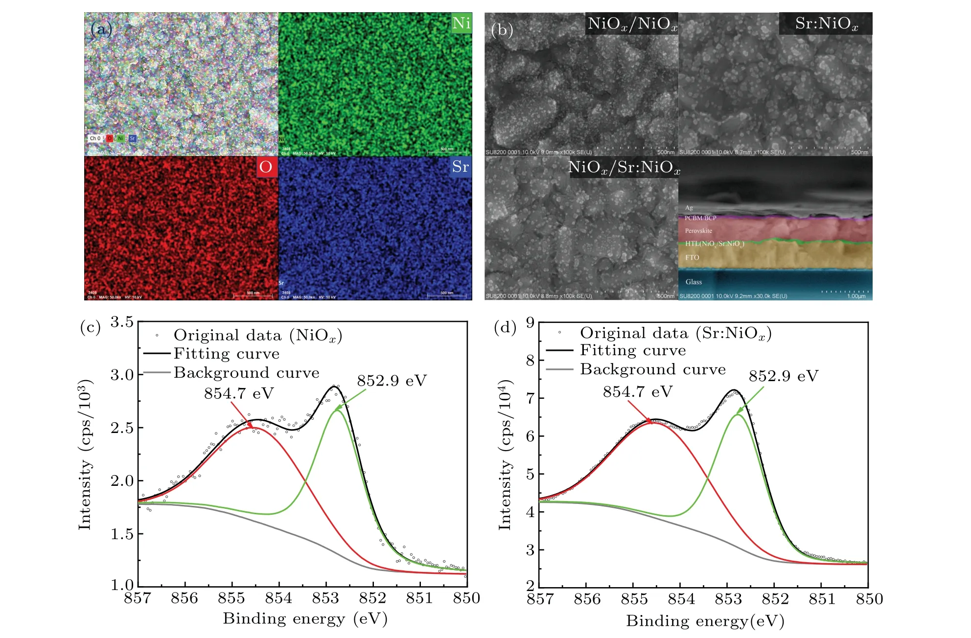
Fig. 1. (a) EDS-mapping spectrum of O, Ni, Sr in Sr:NiOx film. (b) SEM images of NiOx, Sr:NiOx and NiOx/Sr:NiOx films, and SEM cross-section image of the device. XPS spectrum of Ni in(c)NiOx and(d)Sr:NiOx films.
Energy level alignment of NiOx,Sr:NiOx,and perovskite film (PVSK) is important for the analysis of carrier transport from the perovskite active layer to the HTL, so we first used the UV-vis absorption spectra and the UPS(Figs.S5 and S6)to measure the energy level structure of all the functional layers.Through UV-vis measurement, we found that the absorbance of Sr:NiOxand pure NiOxHTL are similar (Fig. S5a), and the calculated band gaps(Eg)are also very close to each other(Fig. S5b). This means that Sr doping does not change light absorbance of the NiOxHTL.Figure S6 shows cut-off energy and valence band edge in NiOx,Sr:NiOxand perovskite thinfilm by UPS measurements,we can further calculate the Fermi level and valence band maximum(VBM)of semiconductors.The work function is the difference between the Fermi level and the vacuum level, so the work function is defined asφ=21.21-Ecutoff.[44]According to the formula,φof NiOxis 5.15 eV,φof Sr:NiOxis 5.21 eV,andφof PVSK is 5.12 eV.The valence band edge is the difference between the Fermi level and the VBM value,so the VBM values of NiOx,Sr:NiOxand perovskite film are-6.00 eV,-6.02 eV, and-6.36 eV,respectively. The energy level structure of hole transport layers and perovskite calculated from the relevant test results is shown in Fig. 2(a). The results indicate that the Fermi energy level decreases with Sr doping. This is consistent with the semiconductor doping law and previously report.[20]We also notice that the Fermi energy level of NiOxis 0.06 eV higher than Sr:NiOx,after contacting of these two films,band bending at the interface will happen and the bending direction is shown in Fig. 2(b), which is helpful for transportation of holes. Moreover, based on the same band bending rules, the photogenerated holes in the perovskite films could also be effectively extracted by the NiOxfilm. Compared to the single layer HTL, the NiOx/Sr:NiOxbilayer HTL could produce an additional driving force for hole transport, which may accelerate carrier transport and inhibit interface recombination at HTL/PVSK.
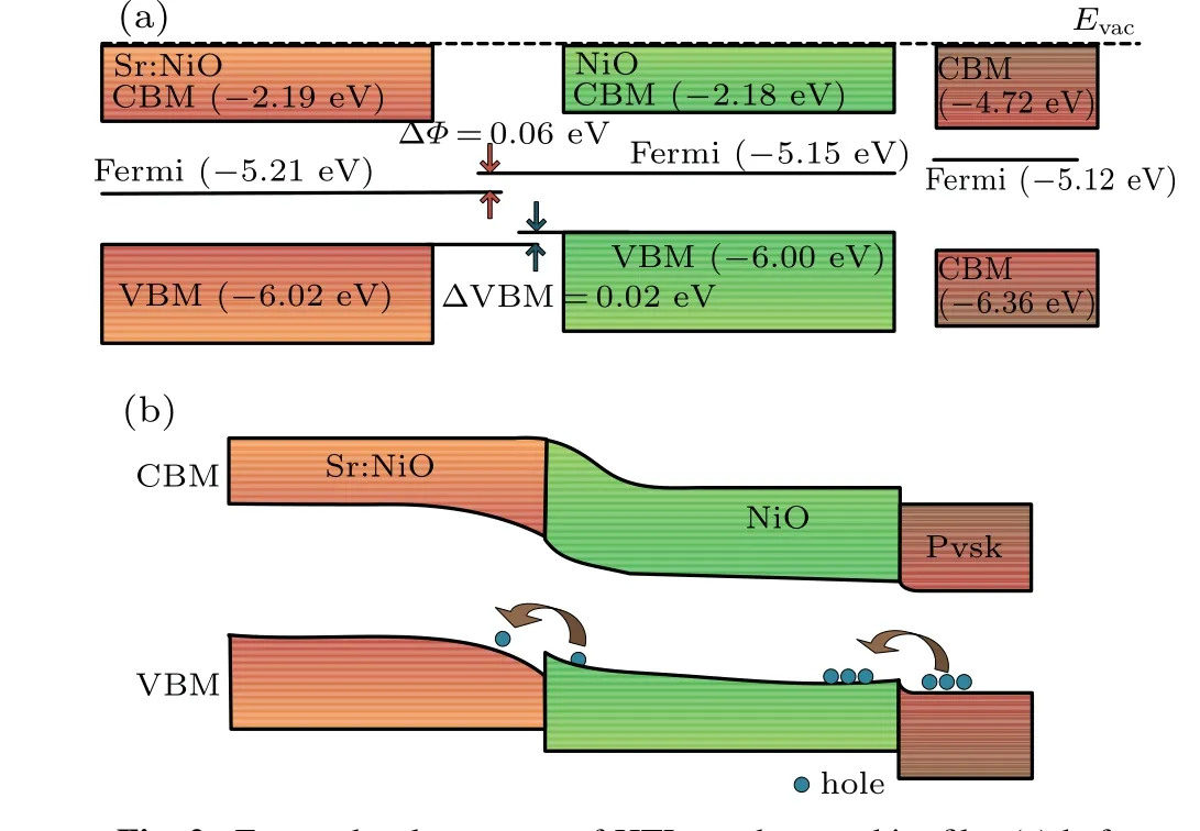
Fig. 2. Energy level structure of HTLs and perovskite film (a) before and (b) after contacting, and the transport of photogenerated holes in different films.
TheJ-Vcurves of PSCs based on different HTLs are presented in Fig. 3, and the corresponding photovoltaic parameters are listed in Table 1. The device using the NiOx/Sr:NiOxbilayer HTL shows the best performance, exhibiting a PCE of 18.44%, aVocof 1.01 V, a short circuit current density(Jsc)of 22.81 mA·cm-2, and a fill factor(FF)of 0.80. Compared to the devices employing single layer HTLs,the device based on the bilayer HTL has evident advantages in all photovoltaic parameters. The result demonstrates that the bilayer HTL could realize our expectations that proper design of energy level alignment in HTL is useful to improve charge transfer and to decrease carrier recombination. Under the driving force of electric field generated in the bilayer HTL, the hole transport efficiency could be greatly improved. Additionally,we find that the device based on the single-layer Sr-doped NiOxHTL could enhance the performance compared to the one using the NiOxHTL, especially on the parameters ofJscand FF because of the better conductivity of the doped film.However, itsVocdoes not increase obviously, which should be ascribed to some additional defects in the Sr:NiOxfilm introduced by the doping process, these defects would play as carrier recombination sites at HTL/perovskite interface. In regard to the NiOx/Sr:NiOxbilayer HTL, the doped film does not directly contact with the perovskite layer,so no additional defects are introduced to the interface. In Fig. 3(a), all the three devices have negligible hysteresis, presenting the advantage of inverted PSCs. The IPCE and integratedJscare shown in Fig. 3(b), the integratedJscdata are close to the values shown in theJ-Vcurves. Figures 3(c) and S7 show the statistic results of PCE,Jsc,Voc, and FF,respectively. We find that the bilayer HTL presents apparent advantage in PCE,Jsc, and FF with higher average values and narrow distribution, compared to the other two HTLs. Figure 3(d) shows the great working stability of the best performance PSC using NiOx/Sr:NiOxHTL without encapsulation,the PCE maintains 89% after 192 h. The effect of Sr concentration in the NiOx/Sr:NiOxbilayer HTL has been investigated,as shown in Fig. S8 and Table S2. The ratio for Sr/Ni is closely related to device performance. As the Sr/Ni increases from 0 to 8%,photovoltaic performance enhances apparently because of the improved electrical property of the Sr:NiOxfilm. However,as the ratio of Sr/Ni reaches 10%,the device performance decreases slightly,which may be induced by the lattice disorder as the over-doping process.

Table 1. Photovoltaic parameters of the champion inverted planar PSCs based on different HTLs.
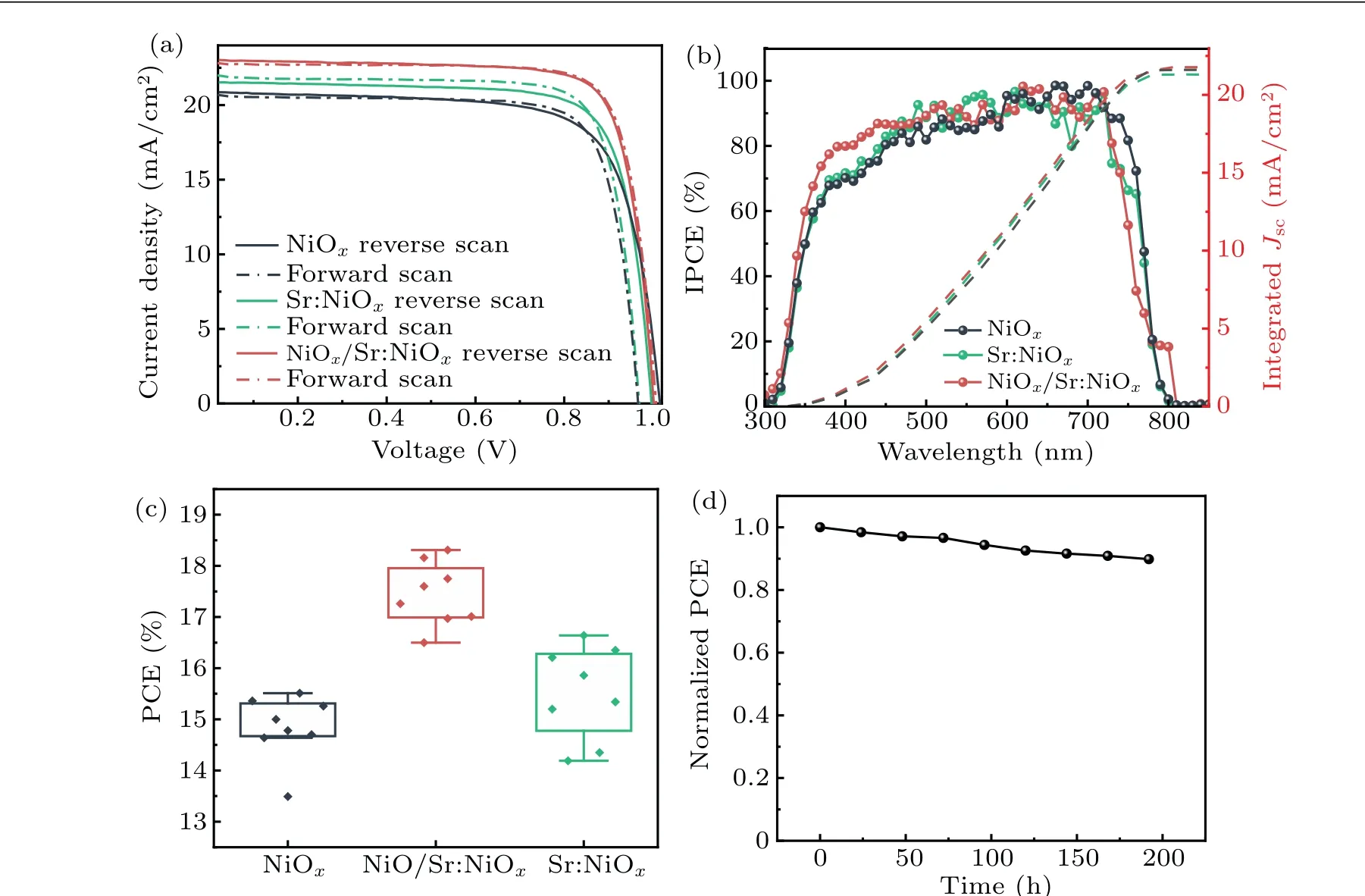
Fig.3. (a)The J-V curves of champion PSCs based on different HTLs under reverse and forward scans. (b)IPCE spectrum and integrated Jsc.(c)Statistic results of PCE of the devices based on varied HTLs. (d)Normalized PCE as a function of time(hour)for best performance PSC using the NiOx/Sr:NiOx HTL without encapsulation.
In order to understand carrier dynamics at interfaces,the film was tested by steady-state photoluminescence (PL). We prepared the samples with the structure of FTO/HTL/PVSK,using the same preparation method as the solar cells. We find that the emission peak of the Sr:NiOx-based film has an overall decrease compared to the emission peak of NiOxbased one, as shown in Fig. 3(a). This decrease may be induced by the better carrier extraction of Sr:NiOxfrom the perovskite film as its enhanced conductivity,but it could also originate from the increased non-radiative carrier recombination as the introduction of additional defects in the Sr:NiOxfilm.However, the emission peak decrease of the NiOx/Sr:NiOxbased film should be induced by the enhanced charge transport and inhibits carrier recombination at the HTL/perovskite interface,because it is NiOxbut not Sr:NiOxthat directly contacts with the perovskite film.[45]Time-resolved photoluminescence spectroscopy (TRPL) is further used to study the charge carrier transport, the curves in Fig. 4(b) can be fitted with the equation

whereτ1andτ2are the life parameters of fast decay and slow decay, respectively. The fast decay process should be attributed to charge transfer at HTL/perovskite interface, and the slow decay should be ascribed to bimolecular radiative recombination.[46]We summarized the life parameters of the devices based on varied HTLs in Table 2. For comparison ofτ1,we know that the value of NiOx/Sr:NiOx-based film is the shortest. A shortτ1value represents effective hole extraction at the HTL/PVSK layer.[47]In addition,the values ofτ2are all above 400 ns,indicating the low level of defects in perovskite films and a slow carrier radiative recombination velocity.

Table 2. Parameters of the TRPL lifetime from fitting curves of themeasurements.
In order to determine the effect of Sr doping on the density of defect states in NiOxfilms, a dark current-voltage(IV) test was performed using the space charge limited current(SCLC)model,as shown in Fig.4(c). We can see that the first half of the linear relationship is in the ohmic region. When the applied voltage exceeds a certain value, the current increases rapidly. The value of the inflection point is named as the trap filled limit voltage (VTFL).[48]Obviously,VTFLof the NiOx/Sr:NiOxfilm is 0.735 V, which is lower than those of both NiOxand Sr:NiOx, indicating a lower density of defect states. The lowVTFLoriginates from the improved charge transfer process at HTL/perovskite interface. Moreover, the recombination mechanism is further studied by measuring the ideal factor associated with a specific recombination characteristic as a function ofVoc. Figure 4(d) shows the dependence of light intensity onVoc. The curve is approximately fitted as a linear function curve. The ideal factors of the devices based on NiOx, Sr:NiOx, and NiOx/Sr:NiOxare 1.64,1.48,and 1.31,respectively. The ideality factor closer to 1 indicates a lower single-molecule Shockley-Read-Hall (SRH)recombination. This result is consistent with the increased FF values by introducing the bilayer HTL,induced by the enhanced charge extraction and decreased carrier recombination at HTL/perovskite interface.[49]Furthermore,EIS delivers carriers transferring and recombination behaviors, as shown in Fig. 4(e). Parameters fitted are summarized in Table S3.The transport resistanceRtr, series resistanceRs, and the recombination resistanceRrecat the interface of PVSK/HTLs are displayed.[47]It can be observed clearly thatRrecof the NiOx/Sr:NiOxbased device increases to 77428 Ω, which is much higher than the others. Compared with the control device,RsandRtrdo not change significantly based on different HTLs. This indicates that NiOx/Sr:NiOxhomojunction HTL devices restrain the recombination at the interface and accelerate the transfer of charge carriers,[48]EIS results are in accordance with the other measurements stated above.
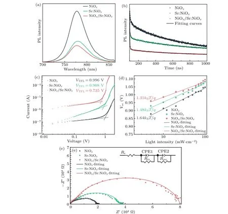
Fig.4. (a)Steady-state photoluminescence(PL)spectra,and(b)transient time-resolved photoluminescence spectrum of FTO/HTL/perovskite.(c)Dark I-V curves of the HTL-only devices. (d)Light intensity dependent Voc for inverted planar PSCs based on different HTLs. (e)Nyquist plots of devices based on different HTLs under a bias of 0.6 V.
4. Conclusion
The bilayer hole transport layer we constructed for inverted planar PSC is composed of NiOx/Sr:NiOx. Sr doping significantly increases the ratio of Ni3+/Ni2+in the Sr:NiOxfilm, thereby increasing its charge transfer property. The Fermi level of Sr:NiOxdecreases compared to NiOxand the band direction after contacting with NiOxcould produce a driving force for holes extracting and reduce the recombination at the interface between the perovskite and HTL layers.Based on this bilayer strategy, we obtain an inverted planar PSC with PCE of 18.44%,Jscof 22.81 mA·cm-2and FF of 0.80,higher than the ones using NiOxor Sr:NiOx. This strategy provides a new idea for the future design of novel hole transport layers,which is effective to make high performance solar cells.
Acknowledgement
This work was supported by the Fundamental Research Funds for the Central Universities, China (Grant No.2021QN1110).
- Chinese Physics B的其它文章
- Surface modulation of halide perovskite films for efficient and stable solar cells
- Graphene-based heterojunction for enhanced photodetectors
- Lithium ion batteries cathode material: V2O5
- A review on 3d transition metal dilute magnetic REIn3 intermetallic compounds
- A low-cost invasive microwave ablation antenna with a directional heating pattern
- A DFT/TD-DFT study of effect of different substituent on ESIPT fluorescence features of 2-(2′-hydroxyphenyl)-4-chloromethylthiazole derivatives

