
Broadband Sequential Load-Modulated Balanced Amplifier Using Coupler-PA Co-Design Approach
2022-02-08 04:26:20RANXiongboDAIZhijiangZHONGKangPANGJingzhouLIMingyu
ZTE Communications 2022年4期
RAN Xiongbo,DAI Zhijiang,ZHONG Kang,PANG Jingzhou,LI Mingyu
(School of Microelectronics and Communication Engineering,Chongqing University,Chongqing 400044,China)
Abstract: The basic theory of the sequential load-modulated balanced amplifier (SLMBA) is introduced and the working principle of its active load modulation is analyzed in this paper.In order to further improve the performance of the SLMBA,a co-designed method of the coupler and power amplifier (PA) is proposed,which is different from the traditional design of couplers.According to the back-off point and saturation point of the SLMBA,this coupler-PA co-design approach can make the working state of the coupler and three-way PA closer to the actual situation,which improves the overall performance of the SLMBA.The maximum output power ratio of the control PA and the balance PA is then determined by the preset output power back-off (OBO) of 10 dB,and the phase compensation line is determined by the trace of the load modulation impedance of the balanced PA.In order to verify the proposed method,an SLMBA operating at 1.5–2.7 GHz (57% relative bandwidth) is designed.The layout simulation results show that its saturated output powers achieve 40.7–43.7 dBm and the small signal gains are 9.7–12.4 dB.Besides,the drain efficiencies at the saturated point and 10 dB OBO point are 52.7%–73.7% and 44.9%–59.2% respectively.
Keywords: SLMBA;broadband;coupler;co-design
1 Introduction
With the advent of the 5G era,modern communication systems often using particularly complex modulation methods result in an increasingly larger peak-to-average power ratio (PAPR),which requires the power amplifier (PA) to keep high efficiency at the output power back-off (OBO) region.Load modulation PAs,as one of the architectures that can efficiently amplify high PAPR signals,have become a research hotspot in recent years.
With the emergence of a large number of new application scenarios,such as portable small base stations and smart wearable devices,the battery capacity determines the output power.Compared with the limited 6 dB OBO of a traditional Doherty PA[1–5],a larger range of OBO is required in these new scenarios.Active load modulation balanced power amplifiers (LMBA),as a new load modulation PA architecture,have great advantages in terms of high efficiency at large OBO and broadband design.They also have great potential in the construction of 5G base stations.
In 2016,SHEPPHARD et al.from Cardiff University,UK proposed a new dual-input PA architecture—LMBA[6].Two directional couplers are used as the input and output networks of the two PAs respectively and the control signal is injected into the balanced PA through the isolated port of the output coupler.LMBA can modulate the load impedance of the balanced amplifier by changing the amplitude and phase of the external control signal to realize high efficiency at OBO.In 2017,PEDNEKAR et al.[7]from the University of Colorado,USA proposed a single-input LMBA architecture based on the traditional LMBA architecture.The output signal of a peaking PA is directly injected into the isolation port of the output coupler as a control signal to realize load modulation of the balanced PA and an octave LMBA which worked at 1.8–3.8 GHz is designed.The maximum output power is 44 dBm and added efficiencies at the 6 dB OBO are 29%–45%.In order to meet the application scenarios of wireless base stations,QUAGLIA et al.[8]of Cardiff University,UK proposed an LMBA architecture using the pre-matching technology and compared the bandwidth and linearity of the proposed structure with the Doherty PA in 2018.An LMBA working in 1.7–2.5 GHz was designed for communication base stations.In 2020,PANG et al.[9]of University College Dublin,Ireland and CAYO et al.[10]of University of Central Florida,USA proposed a new LMBA architecture called Sequential LMBA (SLMBA).The control PA would work in class AB as the carrier PA and the balanced PA would work in class C as a peak PA.Compared with the traditional LMBA,this architecture can achieve a larger range of OBO and higher efficiency in the OBO region.In 2020,PANG et al.[11]also proposed an LMBA that worked in a continuous working mode and realized a continuous output matching network by controlling the phase difference of each PA branch.In 2021,CAO et al.[12]proposed an asymmetric SLMBA architecture,in which the balanced PA was composed of two PAs with different maximum power so that the impedance of the isolated termination of the output coupler was no longer constant.This meant that the control PA also had a load modulation progress and the overdriving of SLMBA was solved.An ALMBA with 0.55–2.2 GHz (relative bandwidth of 120%) was designed and the measured efficiencies at 10 dB OBO were 39%–64%.
Since the first LMBA architecture was proposed in 2016,researchers have conducted a lot of research on it.However,the research generally focuses on application scenarios and architectural innovations and there are few targeted designs for its couplers.In this paper,we will study the co-design of the coupler and PAs for improving the overall performance of SLMBA.
2 Introduction and Theoretical Derivation of SLMBA
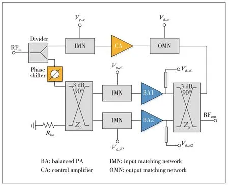
The architecture of SLMBA is shown in Fig.1(a).In this architecture,a class AB amplifier is used as a carrier amplifier,while a balanced PA (BA) is biased in class C as a peaking amplifier.The carrier amplifier is connected to the isolated port of the 90° directional coupler as a control amplifier (CA),while the peaking amplifiers are connected to the through port and the coupling port,respectively.When the phase difference of two peaking amplifiers is 90°,they will become a balanced pair of amplifiers.In the low power region,when the output power is below the power of the predetermined OBO point,the peaking amplifiers are turned off and the output power is only provided by the carrier PA;when the output power is higher than the power of the predetermined OBO point,the two peaking PAs are turned on and the carrier amplifier reaches power saturation.With the further increase of input power,due to the saturation state of the carrier PA,the additional power increase is mainly provided by the peaking PAs.
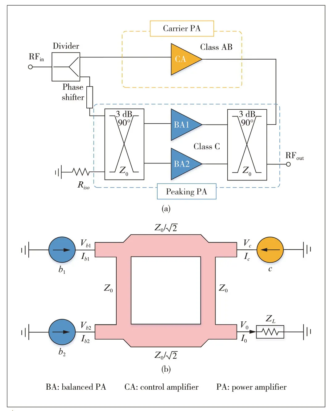
▲Figure 1.(a) Sequential load-modulated balanced amplifier (SLMBA)architecture and (b) active load modulation model of SLMBA
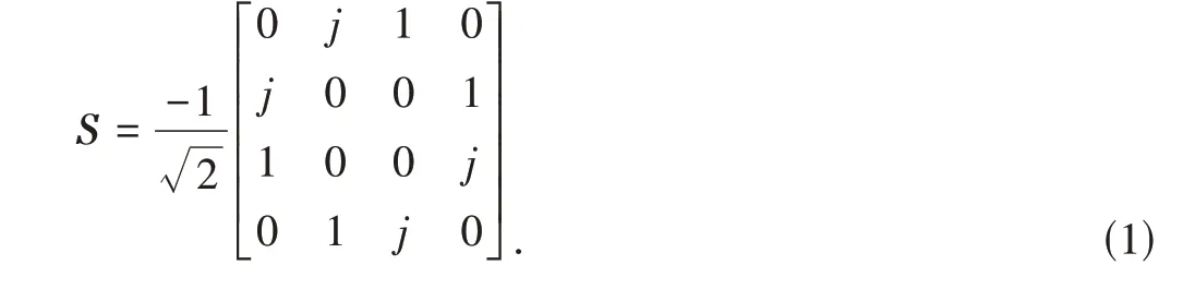
As shown in Fig.1(a),SLMBA consists of a CA and a pair of BAs.The BAs are biased in class C,in which two symmetrical PAs are connected at the input and output of two orthogonal directional couplers and the phase difference of two paths is 90°.A PA working in class AB is used as a CA,and its output signal is injected into the isolated port of the output coupler as a control signal of the SLMBA.The three-way PAs can be regarded as three current sources,which act on the output coupler as an excitation source.The current sourcesb1andb2are two symmetrical balanced PAs and the current sourcecis CA.Fig.1(b) shows the load modulation schematic with an ideal coupler.The normalizedSparameter matrix of the coupler can be directly obtained,as shown in Eq.(1).
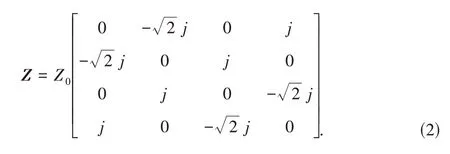
We set the characteristic impedance of the coupler toZ0.According to the conversion relationship of the two-port network,the impedance matrix can be obtained as Eq.(2).
According to Eq.(2),the expression of the load impedance of the balanced PA can be deduced as Eq.(3).
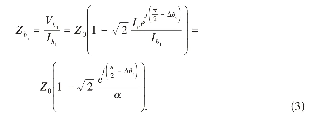
It can be seen from Eq.(3) that the load impedance of the BAs is only related to the characteristic impedanceZ0of the coupler,the current ratio (α),and the phase difference between CA and BAs (ΔθC).Fig.2(a) shows the impedance traces of the BAs and the CA with different phase differences and different output power levels under the OBO of 10 dB.As shown in Fig.2(a),the load impedance of the CA remains constant and is not affected by the output current and output power of the BAs;the load impedances of the BAs are infinite when they are not turned on.However,the values of their load impedance gradually decrease with the increasing output power.It can be seen that the trajectories ofZBAdecrease along the real axis of the Smith chart and finally reach saturation with the increase of output power.Therefore,the theoretical optimal modulation phase difference of SLMBA is -90°.In the design,the phase difference of the two PAs is usually set to -90°.
The power and efficiency of SLMBA are derived below.When the phase difference is fixed as ΔθC=-90°,the output power of the CA and BAs can be deduced as:
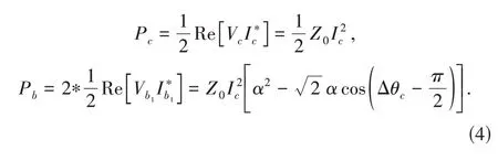
From Eq.(4),the relationship between the output power of SLMBA and the output power of the three PAs can be obtained:
It can be seen from Eq.(5) that the output power of the SLMBA is equal to the sum of the output power of the CA and BAs.Therefore,the efficiency of SLMBA can be expressed as:

After the value of OBO is determined,the current ratioαis also determined.For instance,if the value of OBO is 10 dB,αis 1.53.Fig.2(b) shows the drain efficiency curves of SLMBA at different current ratios.
3 Design of Broadband SLMBA
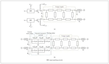
Fig.3 shows the schematic diagram of the broadband SLMBA architecture.The CA works in class AB as the carrier PA.The maximum output power of the BAs is equal,and the BAs work in class C as the peak PA.The output coupler is directly used as the output network of the BAs to avoid SLMBA’s bandwidth being limited by additional output-matching networks.
According to the working principle of SLMBA described in the previous section,amplitude modulation consists of two basic parts: 1) determining the current or power ratio between the BAs and the CA and 2) controlling CA to work in a saturation state and BAs to turn on simultaneously in the power back-off region.
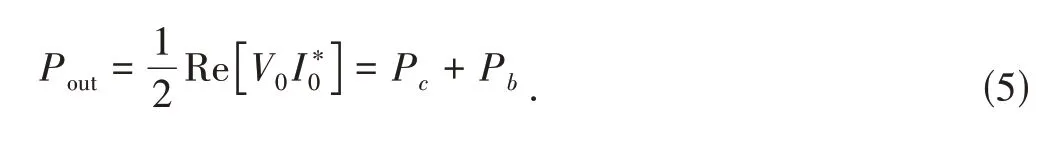
The maximum output power of CA depends on the saturation output power of SLMBA and the OBO level.The relationship between the saturation output power of SLMBA and the preset OBO can be described as:
▲Figure 3.Architecture of broadband sequential load-modulated balanced amplifier (SLMBA)
wherePTotal,SATrepresents the saturation output power of SLMBA,which is the sum of the output power of CA and BAs:

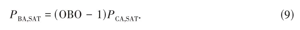
In the actual design process,the preset range of OBO can be realized by selecting BAs and CA transistors with appropriate output power.The CA of this design adopts CGH40010F provided by Wolfspeed and the standard drain voltage is 28 V.However,the drain voltage of the CA is stepped down to 12 V to expand the range of OBO.This can extend the OBO range to 10 dB.The selection of the output power of the BAs is shown in Eq.(9).
Therefore,we chose CGH40010F with a standard output power of 10 W and a drain voltage of 28 V as BAs to achieve OBO=10 dB.Then the gate voltage is controlled to make BAs work in class C and turn on at the preset OBO point.Since the CA is in power saturation in the entire range of OBO,the total output power of the SLMBA depends largely on the output power of the BAs.
According to the theory of SLMBA deduced above,the load impedance of CA in the whole process of SLMBA remains unchanged with infinite isolation of the ideal coupler:

The main bandwidth limitation of a Doherty PA is brought by the inverter network of 90°of the carrier PA.For an SLMBA,the load of the output network of the carrier PA remains unchanged.Therefore,the SLMBA has the potential to extend broadband.Since the load of CA remains unchanged during the whole working process of SLMBA,its design can be directly performed as an independent single PA,which can greatly reduce the design difficulty.
For BAs,the expression of the load impedance is shown in Eq.(3) after they are turned on.It can be seen that the performance depends greatly on the parameters of the coupler,so the design of the coupler is very important for SLMBA.However,in the actual design,the isolation degree of the isolated termination of the coupler will not be ideal,which will cause the output impedance of the isolated termination to fluctuate.So it will seriously reduce the efficiency at the OBO level of the SLMBA.Meanwhile,the load impedances of the coupler’s input ports are influenced by the active BAs instead of any fixed passive load impedance,which also shows that the independent design method of the coupler does not conform to the actual working state of SLMBA.
Therefore,based on the above two aspects,a method for codesign of the coupler and PAs is proposed in this paper.In the proposed method,the OBO and saturation states of SLMBA are designed respectively.The schematic diagram of the proposed SLMBA is shown in Fig.4.In the design of the OBO state,two BAs are directly used as the load condition of the input port of the coupler.On this basis,the output impedance of the isolated termination of the coupler is made constant to reduce the load fluctuation of the control PA for improving the efficiency at the OBO of SLMBA.For the design of the saturated state,the optimal impedance of the transistorRoptand the transistor package parameter network are regarded as the load conditions of the input port of the coupler.On this basis,the parameters such as isolation and coupling of the coupler are designed.The advantage of the proposed codesign approach (Fig.4) makes the operations of the coupler and three PAs closer to the actual situation,which can improve the overall performance of SLMBA.The simulation results of the designed 3-stage coupler are shown in Fig.5.
Then,the phase modulation should be designed.It can be known that the impedance modulation of BAs will have different traces under different phase differences between the CA and BAs.That is to say,the phase difference between the two branches will affect the efficiency of the range of OBO in the whole operating frequencies,so it is significant to control the phase modulation.
Fig.6 shows the impedance modulation traces of BA under the different phase compensation lines at the center frequency of 2.1 GHz.According to the load line of classical class B PAs[12],a purely resistive impedance trace is optimal for its power and efficiency.It can be seen that the impedance trajectory of BA is the closest to the real axis (pure resistance)when the input phase compensation line is 62.5 mm.According to Ref.[13],the slope of the phase compensation required by SLMBA with frequency is basically the same as the microstrip line.Therefore,the SLMBA phase can be greatly compensated in the entire operating frequencies when the input phase compensation line of BA is connected to the 62.5 mm transmission line.
▲Figure 4.Co-design of the coupler and power amplifier (PA): (a) back-off state;(b) saturation state
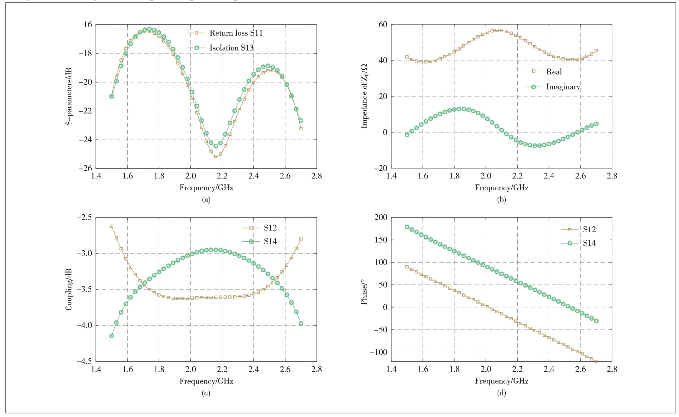
▲Figure 5.Simulation results of the 3-way coupler
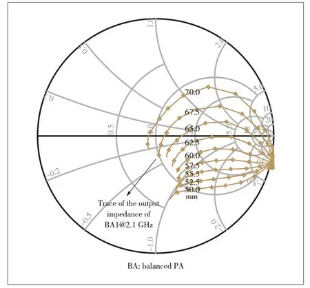
▲Figure 6.Impedance traces of BA1 under different phase compensations
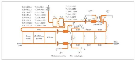
▲Figure 7.Printed circuit board (PCB) structure of the designed sequential load-modulated balanced amplifier (SLMBA)
By debugging the layout of SLMBA,the length of the phase compensation line is set to 60 mm.The printed circuit board(PCB) structure of SLMBA designed by using the proposed codesign method of coupler-PA is shown in Fig.7.The simulation results are shown in Fig.8.The designed SLMBA with 1.5–2.7 GHz (relative bandwidth 57%) has saturated output powers of 40.7–43.7 dBm with saturated drain efficiencies of 52.7%–73.7%,the small signal gain is 9.7–12.4 dB,and the efficiencies are 44.9%–59.2% at 10 dB OBO level.
4 Conclusions
Different from the traditional coupler design method,a codesign approach is proposed for the design of the output coupler and matching network of SLMBA,which improves the performance of SLMBA at the back-off and saturation states.An SLMBA operating at 1.5–2.7 GHz (57% relative bandwidth) is then designed.The layout simulation results show that its saturated output power reaches 40.7–43.7 dBm,the small signal gain is 9.7–12.4 dB,saturated drain efficiency is 52.7%–73.7%,and 10 dB output power back-off efficiency is 44.9%–59.2%.
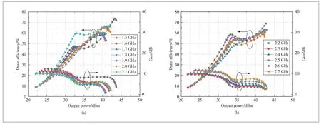
▲Figure 8.Simulation results of the sequential load-modulated balanced amplifier (SLMBA)

- ZTE Communications的其它文章
- ZTE Communications Guidelines for Authors
- Table of Contents,Volume 20,2022
- Physical Layer Security for MmWaveCommunications: Challenges and Solutions
- A Unified Deep Learning Method for CSI Feedback in Massive MIMO Systems
- A Content-Aware Bitrate Selection Method Using Multi-Step Prediction for 360-Degree Video Streaming
- Label Enhancement for Scene Text Detection