Characteristics of Ni-based ohmic contacts on n-type 4H-SiC using different annealing methods
Ziwei Zhou, Weiwei He,,a) Zhenzhong Zhang, Jun Sun, Adolf Sch?ner, and Zedong Zheng
ABSTRACT Nickel is an excellent ohmic-contact metal on 4H-SiC. This paper discusses the formation mechanism of nickel ohmic contact on 4HSiC by assessing the electrical properties and microstructural change. Under high-temperature annealing, the phase of nickel-silicon compound can be observed with X-ray diffraction, and the contact resistance also changes. A comparative experiment was designed to use X-ray diffraction and energy-dispersive spectroscopy to clarify the difference of ohmic-contact material composition and elemental analysis between samples prepared using pulsed laser annealing and rapid thermal annealing. It is found that more Ni2Si and carbon vacancies formed at the interface in the sample prepared using pulsed laser annealing, resulting in a better ohmic-contact characteristic.
? 2021 Author(s). All article content, except where otherwise noted, is licensed under a Creative Commons Attribution (CC BY) license(http://creativecommons.org/licenses/by/4.0/). https://doi.org/10.1063/10.0003763
KEYWORDS Laser annealing, Rapid thermal annealing, Ohmic contact, Ni, 4H-SiC, Carbon vacancy
I. INTRODUCTION
Silicon carbide (SiC) is a wide-bandgap semiconductor material with high thermal conductivity, high breakdown field, highsaturation electron drift velocity, high chemical stability, strong mechanical strength, and other excellent properties, all of which allow the development of high-power electronics applications.1-4Ohmic contact(OC)plays an important role in SiC power devices,with lower OC resistance being effective in reducing device losses and obtaining better performance.5There are many ways to reduce OC resistance, such as by changing the OC metal, changing the annealing process,and adopting special surface treatment technologies.6-8Nickel(Ni)is an excellent OC metal on 4H-SiC.Hanet al.9studied the OC formation mechanism of Ni on n-type 4H-SiC,and herein we study the properties of Ni-based OCs under different annealing processes.
The processes of rapid thermal annealing (RTA) and pulsed laser annealing (PLA) have their own advantages in chip manufacturing, with RTA being relatively inexpensive and widely used.Vassilevskiet al.10deposited 50-nm-thick Ni on SiC and calculated a specific contact resistance(SCR)of 9×10?5Ω cm2after 2 min of annealing at 1000○C. Perezet al.11deposited 100-nmthick Ni and 30-nm-thick Ti layers on SiC and obtained an SCR of 3×10?5Ω cm2after 3 min of annealing at 900○C.Liuet al.12used a 100-nm-thick Ni layer with 1 min of annealing at 975○C in an N2atmosphere and obtained an SCR of 6×10?5Ω cm2.
Most previous research involving RTA has been focused on the OC mechanism and has involved using different contact metals and characterizing the surface morphology.However,wafer processing with RTA is somewhat complicated and involves four steps:(i)contact metal processing on the rear side of the wafer, (ii) Schottky structure formation on the front side, (iii) metal deposition on the rear side, and (iv) passivation layer deposition and curing on the front side. To optimize the process sequence, PLA is introduced,which involves only two steps:(i)Schottky structure formation and passivation on the front side of the wafer,and(ii)contact formation and metal deposition on the rear side.13Under PLA,the rear side of the wafer can be processed after completing the front structure, and the temperature on the rear surface can be greater than 950○C and less than 600○C within 10μm without affecting the metal properties on the front of the wafer.14de Silvaet al.14used a laser density of 4.7 J/cm2to obtain an SCR of 4 × 10?4Ω cm2,Chenget al.15used a laser density of 6 J/cm2to obtained an SCR of 1.97×10?3Ω cm2,and Rascunàet al.16studied Ni-based OCs with laser annealing(4.7 J/cm2)to deal with 4H-SiC and obtained an SCR of 5×10?5Ω cm2.
Herein, we seek to characterize the material composition and element proportions of nickel silicide (Ni2Si) to evaluate which annealing method gives the best OC properties and why.To assess the similarities and differences of Ni/4H-SiC interfaces after RTA and PLA, we use X-ray diffraction (XRD) and energy-dispersive spectroscopy(EDS).
II. EXPERIMENTAL WORK
N-type nitrogen-doped 4H-SiC C-face (0001) bulk substrates with a thickness of 360μm and a doping concentration of 8.0 × 1018cm3were used in the experiments. The samples were cleaned with standard cleaning fluids of RCA,1#,2#,and buffered oxide etchant (BOE) cleaning, then rinsed with deionized water and blow-dried with N2. An Ni layer (100 nm) was deposited on the SiC and heat treated by RTA or PLA under different experimental conditions. Each RTA sample was annealed at 950○C for 2 min in N2ambient, while each PLA sample was treated under the following parameters: the laser wavelength was 355 nm with a 100-μm beam diameter, the laser power was 2.8 J/cm2, and the scanning speed was 660 mm/s. To measure the SCR, the transmission line model (TLM) structure was employed. The fabrication process of the TLM structure can be divided into three steps: (i) remove the excess Ni layer to leave only Ni2Si; (ii) finish the OC photo-etching and deposit an oxide layer; (iii) deposit a Ti/Ni/Ag metal layer by vacuum evaporation and metal photoetching. The TLM model consists of five contact pads (200μm× 60μm) with spacings ofd1= 30,d2= 40,d3= 50, andd4=100μm.
III. RESULTS AND DISCUSSION
A. Results
Through data fitting and calculation of the TLM data for the samples, the SCR values for the PLA and RTA samples were 5.1×10?5and 2.1×10?4Ω cm2,respectively.The XRD data show that the Ni/SiC interface in each type of sample was Ni2Si,and the EDS data show that the PLA sample contained more Ni2Si because of the higher proportions of Ni.Based on the analysis,the PLA sample had more free carbon distributed on the SiC surface, therefore there may have been many carbon vacancies inside the SiC.Both of these phenomena could reduce the OC resistance,which is probably why the PLA sample had the better OC characteristic.
B. Discussion

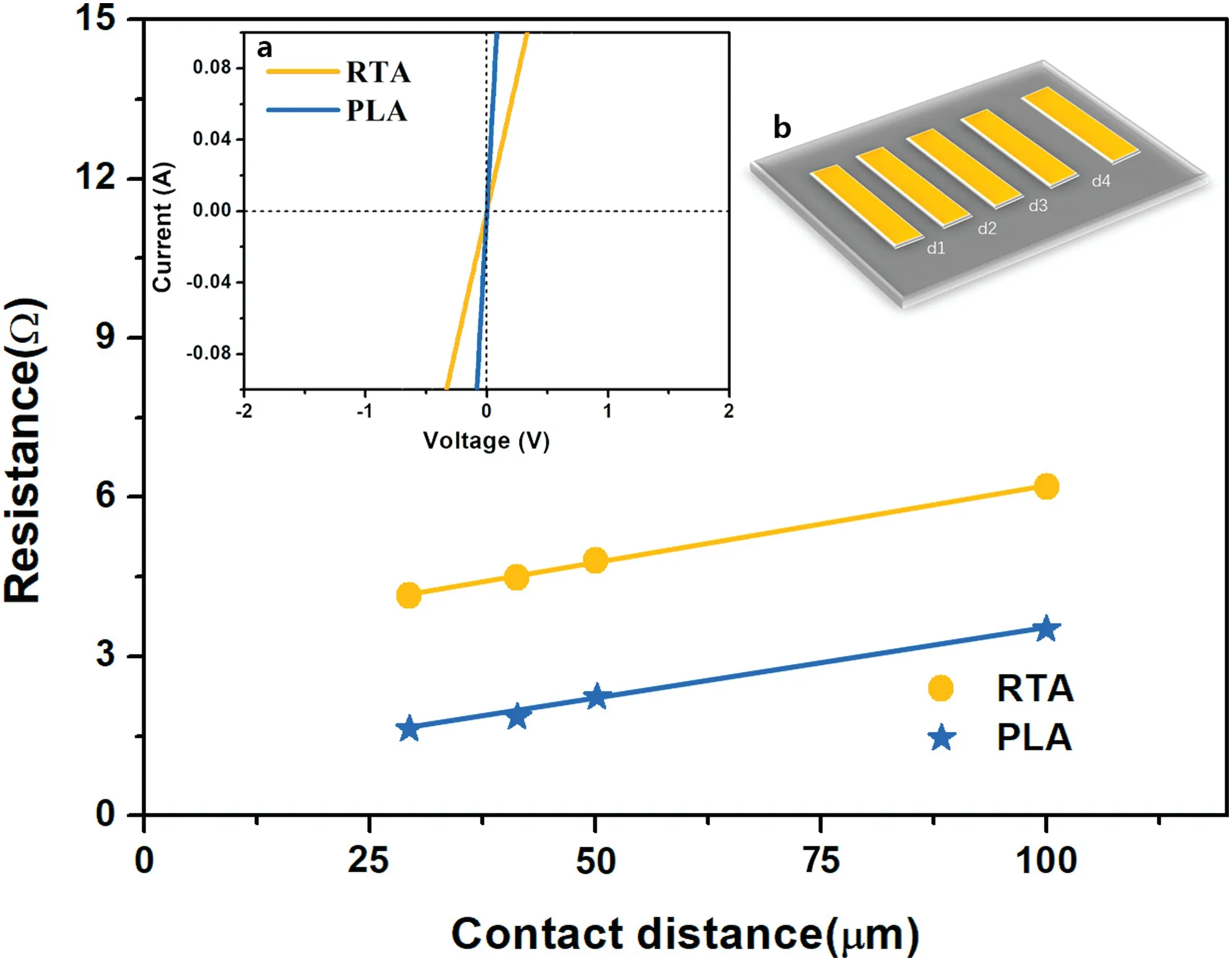
FIG. 1. Total resistance vs contact distance d (30-100 μm) for rapid thermal annealing(RTA)and pulsed laser annealing(PLA)samples.Inset a:I-V curves for d=30 μm.Inset b:schematic of transmission line model(TLM)structure.
A TLM test pattern was prepared to measure the electrical properties of the Ni/SiC contacts on the PLA and RTA samples.As shown in Fig. 1(b), each contact pad of the TLM structure was laterally isolated.17TheI-Vcharacteristic curves (d= 30μm) of the PLA and RTA samples are shown in Fig.1(a),and each annealing method obtained OC characteristics. The SCRRcis calculated from13

where the contact width isZ= 200μm, the contact gapdvaries from 30 to 100μm,andRshis the sheet resistance.According to the test and data fitting ofRtotalvs contact distance in Fig. 1, the PLA sample had the better OC characteristic (OC resistance: 0.428 Ω)than the RTA sample (OC resistance: 1.745 Ω). The SCR values of the PLA and RTA samples were calculated as 5.1 × 10?5and 2.1 × 10?4Ω cm2, respectively. As indicated, for the same wafer processed with different annealing methods, the SCR of the PLA sample was lower than that of the RTA sample. In future work,we will change the PLA parameters (e.g., laser wavelength, beam diameter, laser power, scanning speed) to optimize the interface temperature distribution and obtain better OC quality.

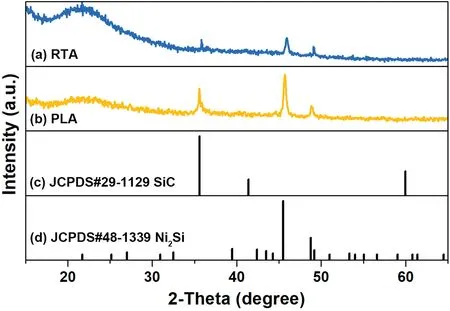
FIG. 2. X-ray diffraction (XRD) patterns for (a) RTA and (b) PLA samples, with standard patterns for(c)SiC JCPDS#29-1129 and(d)Ni2Si JCPDS#48-1339.

FIG.3.Energy-dispersive spectroscopy(EDS)results for(a)PLA and(b)RTA samples.For each spectrum,the inset shows the corresponding sampling region.
We then removed the metal layer to expose the Ni/SiC interface to the surface, and the XRD patterns for the RTA and PLA samples are shown in Figs. 2(a) and 2(b), respectively. The broad peak around 22○in the XRD data for the RTA and PLA samples is because each sample was fixed to the sample table with paraffin.The other diffraction peaks for the RTA and PLA samples belong to SiC(JCPDS#29-1129)and Ni2Si(JCPDS#48-1339).The presence of some low-intensity impurity peaks in the XRD patterns for the RTA and PLA samples might be due to other forms of nickel silicide (e.g., NiSi or NiSi2), but it is clear that Ni2Si is the predominant phase.Note that the diffraction peaks for the PLA sample are much stronger in intensity than those for the RTA sample, which means that the Ni2Si in the PLA sample had better lattice arrangement, and the PLA sample may have had more Ni2Si in its Ni/SiC interface.
To determine whether the PLA sample had more Ni2Si in its Ni/SiC interface,we consider the EDS spectra of the PLA and RTA samples as shown in Fig.3.The integral intensity of the Ni peak for the PLA sample is obviously larger than that for the RTA sample,and the elemental composition ratios(Table I)lead to the same conclusion:the PLA sampling region contained 25.30%Ni,whereas the RTA one contained only 8.33%Ni,which indicates that more Ni2Si was generated in the PLA sample.
According to the literature, the OC characteristic is due to the formation of Ni2Si.18,19During high-temperature annealing,Nireacts with SiC to produce Ni2Si,and at the same time free carbon forms and aggregates in the Ni/SiC interface, free carbon being a highly efficient conductor of electricity.20Therefore,more graphite is distributed in the interface of the PLA sample,so its OC characteristic is better. On the other hand, the free carbon moves to the SiC surface,so there might be many carbon vacancies inside the SiC that can act as donors with positive charges, and the width of the depletion layer and the height of the effective tunneling barrier for electrons transport decrease simultaneously,resulting in the reduction of SCR.21,22Based on these two phenomena, using PLA can enhance the OC characteristic of 4H-SiC devices by lowering the SCR.

TABLE I.Elemental composition ratios[%]in PLA and RTA sampling regions.
IV. CONCLUSIONS
Prepared samples were treated with either PLA(2.8 J/cm2)or RTA(950○C for 2 min).The PLA sample had a better OC characteristic,with an OC resistance of 5.1×10?5Ω cm2,whereas the SCR of the RTA sample was only 2.1×10?4Ω cm2.Material composition and element analysis using XRD and EDS showed that the Ni/SiC interface of the PLA sample contained more Ni2Si, indicating that more carbon clusters and carbon vacancies were produced.Carbon clusters help to increase the conductivity,and carbon vacancies help to increase the tunneling probability.Therefore,using PLA instead of RTA results in 4H-SiC devices with a better OC characteristic with lower SCR.
DECLARATION OF COMPETING INTERESTS
The authors declare that they have no known competing financial interests or personal relationships that could have appeared to influence the work reported in this paper.
ACKNOWLEDGMENTS
This work was supported by Shenzhen Science and Technology Program(Grant No.KQTD2017033016491218).
- 納米技術(shù)與精密工程的其它文章
- Propagation characteristics of photonic crystal fibers selectively filled with ionic liquid
- Deep-learning-based nanowire detection in AFM images for automated nanomanipulation
- A combined virtual impactor and field-effect transistor microsystem for particulate matter separation and detection
- Design of a hexagonal air-coupled capacitive micromachined ultrasonic transducer for air parametric array
- On-site low-power sensing nodes for distributed monitoring of heavy metal ions in water

