High responsivity photodetectors based on graphene/WSe2 heterostructure by photogating effect
Shuping Li(李淑萍), Ting Lei(雷挺), Zhongxing Yan(嚴仲興),Yan Wang(王燕), Like Zhang(張黎可), Huayao Tu(涂華垚),Wenhua Shi(時文華),?, and Zhongming Zeng(曾中明),§
1Suzhou Industrial Park Institute of Services Outsourcing,Suzhou 215123,China
2Nanofabrication Facility,Suzhou Institute of Nano-Tech and Nano-Bionics,Chinese Academy of Sciences,Suzhou 215123,China
3School of Nano Technology and Nano Bionics,University of Science and Technology of China,Hefei 230026,China
4School of Electronics and Information Engineering,Wuxi University,Wuxi 214105,China
Keywords: WSe2,heterostructure,photodetector,photogating effect
1.Introduction
Photodetectors based on transition metal dichalcogenides(TMDCs)such as MoS2and WSe2have received much attention due to their flexible structure,[1,2]tunable bandgap,[3,4]and high absorption coefficient.[5,6]Previous studies have demonstrated that the photodetection efficiency of monolayer MoS2and WSe2photodetectors is as low as a few hundred mA/W, due to the light absorption limitations and the effects of non-optimal contact at the metal electrode and material interface.[7,8]Therefore, to obtain high-performance photodetectors, many researchers have turned to heterostructures based on graphene/TMDCs to prepare low-resistance devices.[9–11]Moreover, graphene-based heterostructures retain the inherent photoelectronic properties of a single material due to weak van der Waals forces between layers and the lack of surface dangling bonds, which can further improve device performance.[12–15]For example, Tanet al.and Yehet al.reported that the photodetection efficiency of WSe2and WS2photodetectors increased to 350 A/W and 3.5 A/W,respectively,by using graphene as a transparent contact electrode.[16,17]
The tungsten disulfide (WSe2) has a tunable bandgap(1.2 eV–1.67 eV), bipolar transport behavior, and excellent photoelectronic properties, and has been widely studied as a potential candidate for next-generation optoelectronic devices, such as solar cells, photodetectors, and photonic modulators.[18–21]In addition, graphene can achieve wideband photodetection from ultraviolet to terahertz wavelengths due to its unique zero bandgap structure.[22,23]Furthermore, graphene-based photodetectors exhibit super-fast response speeds due to their ultra-high carrier mobility.[24]Unfortunately, the light absorption efficiency of monolayer graphene is only about 2.3% and usually lacks high photoresponsivity.[25]To generate higher photocurrent, it is possible to construct an internal electric field to separate photo-generated electron–hole pairs, thereby extending the carrier lifetime.[10,26]Therefore,by fabricating a vertical heterostructure device and combining the advantages of WSe2and graphene, it is promising to improve the overall performance of the photodetector.
In the present research,we fabricated a high photodetection efficiency photodetector based on a graphene/WSe2vertical heterostructure.The device covered a layer of high lightabsorbing WSe2material on the graphene channel,which significantly enhanced the device’s light absorption.At the same time,we used the localized grating layer formed by the WSe2material to regulate the carrier concentration of the underlying graphene.At room temperature, the external quantum efficiency of the device reached 1.3×10⁷%,and the photodetection efficiency reached 3.85×10⁴A/W,which is 2–3 orders of magnitude higher than that of the WSe2photodetector.These results demonstrate that using WSe2material as the localized grating layer is an effective way to achieve high photoresponsivity and high external quantum efficiency.
2.Experimental details
2.1.Device fabrication
The graphene/WSe2vdW heterostructure was fabricated using mechanical exfoliation technique.First, few layers graphene flake was exfoliated using 3M tape.Next, the graphene device was fabricated using layout design software(L-edit), electron beam lithography, and electron beam evaporation processes.Finally, WSe2thin film material is obtained through mechanical exfoliation and transferred onto the previously fabricated graphene device, resulting in the graphene/WSe2vertical device.
2.2.Device characterization
The morphology and thickness of the graphene/WSe2vdW heterostructure were measured using an atomic force microscope(AFM).The quality of the heterostructure device was characterized using a Raman spectrometer with a laser wavelength of 532 nm.The photoelectric performance was measured using a semiconductor parameter analyzer (Keithley 2400 and 2612B)in a dark room at room temperature and a laser source with a tunable wavelength of 365 nm–965 nm.
3.Results and discussion
3.1.Device structure and microscopic characterization
Figure 1(a) shows a schematic diagram of the graphene/WSe2vertical heterostructure device on an Si/SiO2substrate.The device is obtained by mechanically exfoliating WSe2thin film material and transferring it onto a previously fabricated graphene device.Figure 1(b) shows an optical image of the graphene/WSe2heterostructure, where WSe2is used as the light-absorbing layer and the localized grating layer, and graphene as the conductive channel layer.The built-in electric field between graphene and WSe2can enhance the separation of electron–hole pairs and reduce the recombination probability.The morphology and thickness of the heterostructure device were characterized by atomic force microscopy (AFM).Figure 1(c) shows the AFM image of the graphene/WSe2vertical heterostructure device,where the orange dashed line represents WSe2, the red dashed line represents graphene, and the scale bar is 10 μm.The thickness information of the graphene/WSe2heterostructure device was extracted from the inset, where the thicknesses of WSe2and graphene were 11 nm and 7 nm,respectively.
Figure 1(d)shows the Raman spectroscopy characterization results of the WSe2and the graphene/WSe2heterostructure region.For the pristine WSe2material, the Raman spectrum exhibits three prominent peaks: E2gat 249 cm?1,2LA(M) at 257 cm?1, and B2gat 308 cm?1, respectively.The Raman spectrum of the graphene/WSe2heterostructure region shows an additional characteristic peak of graphene at 1582.5 cm?1.This G peak originates from the E2gphonon mode,and the two-dimensional(2D)vibration mode’s characteristic peak is located at 2715.6 cm?1,corresponding to double phonon resonance.In the heterostructure region,the signal peak of graphene is much weaker than the Raman intensity of the WSe2material, due to the fact that the WSe2material is covered on top of graphene, causing it to receive much less Raman laser power.
3.2.Electrical characterizations of the graphene/WSe2 heterostructure device
Figures 2(a) and 2(b) show the output characteristics of the WSe2/h-BN heterostructure device at different gate voltages(Vg).As theVgincreases from 0 V to 50 V,the source–drain current(Ids)also increases,and the output characteristics exhibit a sub-linear behavior due to the Fermi level pinning effect between the metal electrode and the thin film material,as shown in the logarithmic coordinate plot in Fig.S1.As theVgvaries from?60 V to?10 V,the overall magnitude of theIdsincreases with the increase of theVg,corresponding to the transfer characteristic curve shown in Fig.S2, indicating that the WSe2/h-BN heterostructure device exhibits bipolar semiconductor characteristics.The electric field mobility(μFE)of the WSe2/h-BN heterostructure device is calculated using the following formula:
whereμis the mobility of the device,Lis the channel length (5.4 μm),Wis the channel width (8.3 μm),εrepresents the vacuum permittivity (8.854×10¹²F/m),εrrepresents the relative permittivity of the material (3.9 for SiO2and 3.5 for h-BN), anddrepresents the thickness of SiO2(300 nm).Based on Eqs.(1)and(2),the electron(hole)mobility of the WSe2/h-BN heterostructure device at a source–drain voltage (Vds) of 1 V can be calculated as 7.20 cm2·V?1·s?1(25.17 cm2·V?1·s?1).

Fig.2.Electrical characteristics of WSe2/h-BN heterostructure device and graphene/WSe2 heterostructure device under dark conditions.(a) Output characteristic curve of WSe2/h-BN heterostructure device with gate voltage ranging from 0 V to 50 V; (b) output characteristic curve with gate voltage ranging from ?60 V to ?10 V; (c) output characteristic curve of graphene/WSe2 heterostructure device with gate voltage ranging from 0 V to 90 V;(d)output characteristic curve with gate voltage ranging from ?90 V to 0 V.
Figures 2(c) and 2(d) show the output characteristics of the heterostructure device as theVgvaries from 0 V to 90 V and from?90 V to 0 V,respectively.The results indicate Ohmic contact between graphene and the metal electrode without a Schottky barrier.The concentration of graphene conductive channel can be controlled by theVg.As theVgincreases from 0 V to 90 V,theIdsincreases.Conversely,as theVgincreases from?90 V to 0 V,theIdsdecreases.This is consistent with the transfer characteristics curve shown in Fig.S3, demonstrating the bipolar semiconductor behavior of the heterostructure device.
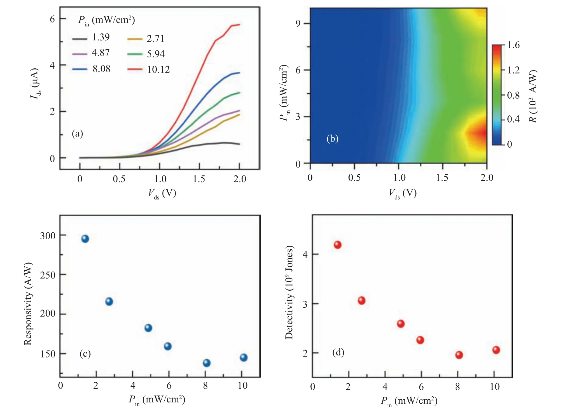
Based on the above outstanding electrical performance,we further investigated the photodetection performance of WSe2/h-BN heterostructure devices.Figure 3(a) shows the output characteristics of the heterostructure device under visible light irradiation at 532 nm, withPinvalues ranging from 1.39 mW/cm2to 10.12 mW/cm2.As can be seen, the heterostructure device exhibits a large photocurrent at various light power densities, and the photocurrent increases with increasingPinvalues.WhenPinis 10.12 mW/cm2, theIdscan reach 5.74×10?6A, which is more than 5 μA higher than that under dark conditions.Figure 3(b) shows the dependence of the responsivity of the heterostructure device on theVdsand the incident light power density.The results show thatRsharply increases with increasing theVds, and reaches a maximum value of 1535.05 A/W atPin= 2.71 mW/cm2andVds=2 V.Figures 3(c) and 3(d) show the incident light power distribution curves of theRandD?of the heterostructure device,demonstrating good response characteristics of the WSe2/h-BN heterostructure device at various light power densities.Among them, whenPinis 1.39 mW/cm2and theIdsis 1 V, theRandD?can reach the highest values, which are 295.12 A/W and 4.19×10⁹Jones,respectively.
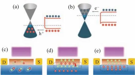
Next, we will delve into the photogating effect in the graphene/WSe2vertical heterostructure device and its origin, as shown in Fig.4(a).Taking the example of the graphene/WSe2vertical heterostructure device operating at a gate voltage ofVg<0 V,when WSe2and graphene come into contact with each other, due to the difference in carrier concentration and Fermi level,the holes in WSe2will diffuse towards graphene under the effect of carrier concentration gradient.Finally, under no external voltage, the diffusion and drift motions of the charge carriers are balanced, achieving dynamic equilibrium.In this state, an intrinsic electric field pointing from WSe2to graphene is generated in the depletion layer formed between them.By changing the external voltage,the width of the depletion layer and the strength of the intrinsic electric field can be further adjusted,thereby achieving the tuning of the heterostructure device’s performance.

Fig.3.WSe2/h-BN heterostructure device: (a) output characteristic curves under different incident light intensities in dark conditions (wavelength λ =532 nm,Vg=0 V);(b)the 2D relationship between photoresponsivity and incident light power density and source–drain voltage(λ =532 nm,Vg=0 V);the variation of(c)photoresponsivity and(d)specific detectivity with incident light power density.

Fig.4.Graphene/WSe2 vertical heterostructure device.Energy band diagrams of graphene/WSe2 vertical heterostructure devices under different gate voltages: (a) Vg <0 V and (b) Vg >0 V (with fixed incident wavelength of 365 nm, red represents holes and dark blue represents electrons);the schematic diagrams of(c)generation, (d)transfer, and(e)confinement of photoexcited electron–hole pairs.The upper layer is made of WSe2 material,the lower layer is made of graphene material,green circles represent electrons,red circles represent holes.
Under dark conditions, the majority of theIdsin heterostructure devices comes from holes in graphene.When a 365-nm wavelength laser is irradiated on the heterostructure device,photo-generated electron–hole pairs are excited in both WSe2and graphene materials, as shown in Fig.4(c).Due to the formation of a built-in electric field from graphene to WSe2at the interface, the photogenerated electron–hole pairs are separated and move towards each material under the influence of the built-in electric field.Specifically,the holes in WSe2are transferred to the underlying graphene layer,while the photogenerated electrons in graphene are transferred to the upper WSe2layer,as shown in Fig.4(d).This process increases the hole concentration in the graphene conductive channel,and the holes drift under the influence of theVds,contributing to the increment of the photocurrent.In addition,due to the existence of the built-in electric field in the heterostructure device, the electrons transferred from graphene are confined to the WSe2layer, as shown in Fig.4(e).This confinement of electrons in the WSe2layer produces a modulation effect similar to the gate voltage.Under this strong coupling effect,electrons in the WSe2layer induce more holes to be generated in the graphene layer,thereby increasing the carrier concentration in the channel and improving the photo-detection performance of the heterostructure device by an order of magnitude.
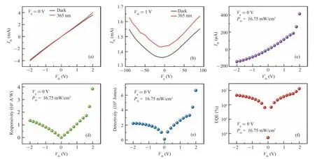
Based on the research of the electrical characteristics of heterostructure devices and the photoelectric properties of WSe2transistors,we continued to test the photo-detection performance of graphene/WSe2heterostructure devices under different conditions.When theVgwas 0 V,we tested the output characteristic curve of the heterostructure device under dark conditions and 365-nm incident wavelength light illumination,as shown in Fig.5(a).With the increase of theVds,the photoelectric current of the heterostructure device also increased,indicating that the collection efficiency of photo-generated carriers gradually improved.At the same time, we also tested the transfer characteristic curve of the heterostructure device under dark conditions and 365-nm incident wavelength light illumination with a fixedVdsof 1 V,as shown in Fig.5(b).It can be seen that the photoelectric current of the heterostructure device under theVgregulation shows a trend of decreasing first and then increasing,indicating that the heterostructure device has bipolar semiconductor characteristics consistent with the experimental results under dark conditions.

Fig.5.Graphene/WSe2 vertical heterostructure device: (a) output characteristics under dark and 365-nm wavelength light illumination (Vg = 0 V);(b) transfer characteristics under dark (Vds =1 V); (c) extracted photocurrent as a function of Vds (Vg =0 V, λ =365 nm); (d) the relationship between responsivity R,(e)detectivity D?,and(f)external quantum efficiency(EQE)with Vds.
Figures 5(d)and 5(e)show the curves ofRandD?of the graphene/WSe2vertical heterostructure device as a function of source–drain voltage (Vds), respectively.The results indicate that theRandD?values of the device also increase with the increase ofVds.TheRandD?of the heterostructure device can be expressed by the following equations:[27–31]
wherePin,A,andeare the incident optical power density,effective illuminated area,and electron charge.
When the device is illuminated with 365-nm wavelength light at a power density of 16.75 mW/cm2and the source–drain voltage is 1 V,RandD?reach 1.34×10⁴A/W and 2.21×10⁹Jones,respectively.When the source–drain voltage is further increased to 2 V,theRandD?of the device are improved to 3.85×10⁴A/W and 6.62×10⁹Jones,respectively.In addition, to further improve the photoresponsivity of the heterostructure device, the gate voltage of the device can be increased to adjust the carrier concentration in the conductive channel.Furthermore, figure 5(f) demonstrates the variation of external quantum efficiency (EQE) with different source–drain voltages.The EQE is a dimensionless quantity that represents the ratio of collected electrons to incident photons in a device,and can be calculated using the following formula:
whereRis the photoresponsivity,his the Planck constant(6.63×10?34J·s),λrepresents the wavelength of the incident laser,andcis the speed of light in vacuum.For the heterostructure device,the EQE reaches 4.6×10⁴%at a source–drain voltage of?2 V.Continuing to increase the voltage to?2 V, the EQE increases to 1.3×10⁷%, indicating that the light absorption efficiency can be improved by changing the source–drain voltage of the device.Finally,This is also comparable to those in previous works (supporting information,Table S1).
4.Conclusion
In summary, we demonstrated a graphene/WSe2vertical heterostructure based highly sensitive photodetector, where the WSe2layer plays a dual role of both the light absorption layer and the localized grating layer.The graphene conductive channel is induced to produce more charge carriers by capacitive coupling.Under the strong photogating effect,graphene/WSe2vertical heterostructure exhibits excellent optoelectronic properties at room temperature, with a detectivity and external quantum efficiency of 6.62×10⁹Jones and 1.3×10⁷%,respectively.Furthermore,the photoresponsivity reaches 3.85×10⁴A/W,which is two to three orders of magnitude higher than that of theWSe2photodetector.
Acknowledgements
Project supported by the National Natural Science Foundation of China (Grant No.11974379), the National Key Basic Research and Development Program of China (Grant No.2021YFC2203400), and Jiangsu Vocational Education Integrated Circuit Technology “Double-Qualified” Famous Teacher Studio(Grant No.2022-13).
- Chinese Physics B的其它文章
- High responsivity photodetectors based on graphene/WSe2 heterostructure by photogating effect
- Progress and realization platforms of dynamic topological photonics
- Shape and diffusion instabilities of two non-spherical gas bubbles under ultrasonic conditions
- Stacking-dependent exchange bias in two-dimensional ferromagnetic/antiferromagnetic bilayers
- Controllable high Curie temperature through 5d transition metal atom doping in CrI3
- Tunable dispersion relations manipulated by strain in skyrmion-based magnonic crystals

