Design and Synthesis of Acceptor-Donor-Acceptor Type Non-Fullerene Acceptors Using Oxindole-Based Bridge for Polymer Solar Cells Applications
GUO Yuqing(郭雨晴), HUANG Jun(黃 峻), LI Zheng(李 正), WU Hongbo(吳宏波), WANG Jing(王 靜), TANG Zheng(唐 正), MA Zaifei(馬在飛), WANG Ming(王 明)*, ZHU Zhijia(朱智甲)*
1 Key Laboratory of Science and Technology of Eco-Textiles, Ministry of Education, College of Chemistry, Chemical Engineering & Biotechnology, Donghua University, Shanghai 201620, China 2 Center for Advanced Low-dimension Materials, State Key Laboratory for Modification of Chemical Fibers and Polymer Materials, College of Materials Science and Engineering, Donghua University, Shanghai 201620, China
Abstract: Two acceptor-donor-acceptor(A-D-A)type non-fullerene acceptors(namely WH1 and WH7)containing the oxindole-based bridge are designed and synthesized for polymer solar cells(PSCs)applications. The bridge unit is introduced through a precursor(6-bromo-1-octylindoline-2,3-dione)that contains both bromine and carbonyl and provides the feasibility of the Pd-catalyzed cross-coupling reaction and the Knoevenagel condensation, respectively. This facile synthetic approach exhibits the potential to gain high performance non-fullerene acceptors through extending π-conjugated backbone with strong light-absorbing building blocks. The synthesis and properties of WH1 and WH7 are demonstrated with different endcap units, then PSCs are fabricated using PBDB-T:WH1 and PBDB-T:WH7 as the active layers, and attain an average power conversion efficiency(PCE)of 2.58% and 6.24%, respectively. Further device physics studies afford the deep insight of structure variation influence on the device performance. This work provides a facile non-fullerene acceptor design strategy and shows how structure variations impact the PSC performance.
Key words: non-fullerene acceptor; polymer solar cell(PSC); conjugated molecules; donor-acceptor(D-A); narrow bandgap
Introduction
Polymer solar cells(PSCs)are under intensive studies due to their advantages of low-cost, light-weight, flexibility, and solution-processed production[1-2].High performance PSCs usually employ a bulk-heterojunction device structure, in which the active layer is a blend ofp-type andn-type semiconductors[3].Forp-type semiconductors, conjugated polymers with donor-acceptor(D-A)alternating fashion have been well-developed and played a key role in the PSC applications[4-5].Forn-type semiconductors, fullerene and its derivatives[6-7]have governed the field until the naissance of fused-ring electron acceptors, such as 3,9-bis(2-methylene-(3-(1,1dicyanomethylene)-indanone))-5,5,11,11tetrakis(4-hexylphenyl)-dithieno[2, 3-d∶2′, 3′d′]-s-indaceno[1, 2-b∶5, 6-b′]dithiophene(ITIC)[8]and(2, 2′-((2Z, 2′Z)-((12, 13-bis(2-ethylhexyl)-3, 9-diundecyl-12,13-dihydro-[1,2, 5]thiadiazolo[3, 4-e]thieno[2,"3″∶4′, 5′]thieno[2′,3′∶4,5]pyrrolo[3, 2-g]thieno[2′,3′∶4, 5]thieno[3, 2-b]indole-2,10-diyl)bis(methanylylidene))bis(5,6-difluoro-3-oxo-2,3-dihydro-1H-indene-2,1-diylidene))dimalononitrile)(Y6)[9], driving the PCEs increasing to above 10%[10-11].Due to the development of non-fullerene acceptors[12-14], the performance of PSCs has climbed up to a new stage with the PCEs going up to about 8%[15-17].These non-fullerene acceptors display strong absorption coefficients in the visible and near-infrared(IR)light region.Moreover, their devices exhibit small energy losses(Eloss)[18-20], which enable PSCs to gain large short-circuit current(Jsc)and open-circuit voltage(Voc)simultaneously.In addition, non-fullerene acceptors also show the low synthesis cost, flexible molecular design and structure modifications, as well as good thermal and photochemical stabilityin comparison with fullerene derivatives[21].

1 Experiment
1.1 Synthesis
Figure 1 shows the molecular design strategy of A-D-A type non-fullerene acceptors using oxindole-based bridge.
Figure 2 shows the detailed synthetic routes of WH1 and WH7.The center donor core precursor M1 was firstly prepared.4, 4, 9, 9-Tetrakis(4-hexylphenyl)-4, 9-dihydro-s-indaceno[1, 2-b∶5, 6-b′]dithiophene was deprotonated byn-butyllithium and then the stannylation was carried out by adding trimethyltin chloride, to give the center core intermediate.The bifunctional intermediate of bridge precursor 6-bromo-1-octylindoline-2, 3-dione was prepared from 6-bromoisatin and 1-bromooctylane under the potassium carbonate in DMF solution.Then the Stille coupling reaction was carried out using 6-bromo-1-octylindoline-2, 3-dione and M1 under the catalytic Pd(PPh3)4in toluene solution to give compound M2.Finally, two target acceptor molecules WH1 and WH7 were obtained from M2 and 3-ethylrhodanine and 2-(3-ethyl-4-oxothiazolidin-2-ylidene)malononitrile, respectively, under a common Knoevenagel condensation condition of triethyl amine as the catalyst and chloroform as the solvent.
The crude product of WH1 was purified by column chromatography, affording the pure compound WH1 as a green solid with a yield of 81%(437 mg, 0.25 mol).The melting point(m.p.)>280 ℃.1H NMR(400 MHz, CDCl3, 298 K): 8.98(d,J=8.4 Hz, 2H), 7.46(s, 2H), 7.38(s, 2H), 7.33(dd,J1=8.4 Hz,J2=1.6 Hz, 2H), 7.26(d,J=8.3 Hz, 8H), 7.21(d,J=8.1 Hz, 8H), 7.01(s, 2H), 4.24(dd,J1=14.1 Hz,J2=6.9 Hz, 4H), 3.80(t,J=7.2 Hz, 4H), 2.58(t,J=7.8 Hz, 8H), 1.73-1.69(m, 4H), 1.65-1.56(m, 8H), 1.42-1.19(m, 50H), and 0.94-0.80(m, 18H).

Fig.1 Molecular design strategy of A-D-A type non-fullerene acceptors using oxindole-based bridge
The crude product of WH7 was purified by column chromatography, affording the pure compound WH7 as a green solid with a yield of 86%(482 mg, 0.27 mol), and the m.p.is more than 280 ℃.1H NMR(400 MHz, CDCl3, 298 K): 8.84(d,J=8.4 Hz, 2H), 7.48(s, 2H), 7.41(s, 2H), 7.35(dd,J1=8.4 Hz,J2=1.6 Hz, 2H), 7.23(d,J=8.1 Hz, 8H), 7.13(d,J=8.2 Hz, 8H), 7.03(s, 2H), 4.31(dd,J1= 14.2 Hz,J2=7.0 Hz, 4H), 3.81(t,J=7.2 Hz, 4H), 2.58(t,J=7.8 Hz, 8H), 1.74-1.70(m, 4H), 1.60(m, 8H), 1.45-1.19(m, 50H), 0.94-0.83(m, 18H).The process of synthesis is shown in Fig.2.
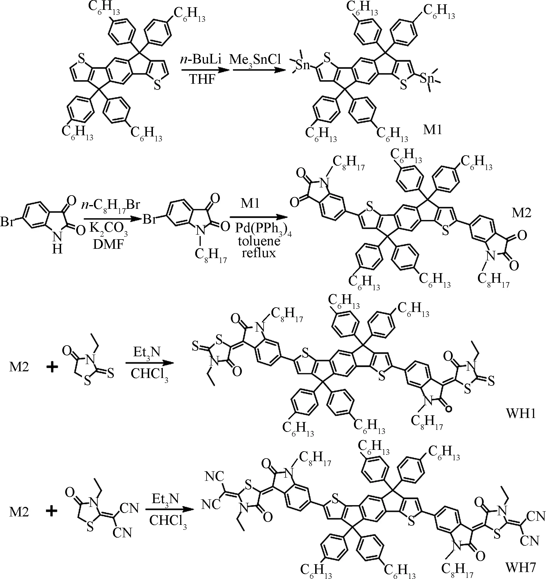
Fig.2 Synthetic routes of WH1 and WH7
1.2 Preparation of PSC devices
Solar cells were fabricated using a conventional device structure comprising which is indium tin oxid(ITO)/PEDOT:PSS/active layer/PFN-Br/Ag, where PEDOT:PSS is poly(3,4-ethylenedioxythiophene)doped with polystyrene sulfonate.Specifically, approximately 40 nm of PEDOT:PSS was deposited as a thin film atop indium tin oxide(ITO)coated glass substrates.The activelayers(PBDB-T:WH1 or PBDB-T:WH7)were spin-coated, followed by spin-casting of PFN-Br(5 nm)and evaporating of silver(40 nm), where PBDB-T is poly[(2,6-(4,8-bis(5-(2-ethylhexyl)thiophen-2-yl)-benzo[1, 2-b∶4,5-b′]dithiophene))-alt-(5,5-(1′,3′-di-2-thienyl-5′,7′-bis(2-ethylhexyl)benzo[1′,2′-c∶4′,5′-c′]dithiophene-4,8-dione))])and PFN-Br is poly(9,9-bis(3′-(N,N-dimethyl)-N-ethylammoinium-propyl-2,7-fluorene)-alt-2,7-(9,9-dioctylfluorene)dibromide)[26].A preliminary screening of active compositions and deposition conditions were carried out.Both PBDB-T:WH1 and PBDB-T:WH7 weight ratios were tested by 1.0∶0.8, 1.0∶1.0, 1.0∶1.5, and 1.0∶2.0, and the 1.0∶1.0 combination performed best among these conditions.The total concentration of blend solutions was 22 mg/mL(chlorobenzene as the solvent), and the spin-cast speed was set to 3 000 r/min, films were annealed under the chlorobenzene vapor for 10 min and then annealed at 150oC for 10 min, which provided the best performance.The active layer thickness was approximately 110 nm.The average performance was calculated from about 40 devices.
Additionally, to investigate the charge transport properties in the PSC device, we measured the hole mobility and electron mobility of PBDB-T:WH1 and PBDB-T:WH7 devices using space-charge limited current(SCLC)model based on their optimal film processing condition[27].The hole-only device structure is ITO/PEDOT:PSS/active layer/MoO3/Ag and the electron-only device structure is glass/ITO/ZnO/active layer/PFN-Br/Ag, respectively.The hole and electron mobilities are calculated by
(1)
whereε0is the absolute dielectric constant,εris the relative dielectric constant,μis the mobility,Vis the applied voltage,Vbiis the build-in voltage, andLis the active layer thickness.SCLC devices were prepared in two different thicknesses to better estimate the mobility.
2 Results and Discussion
2.1 Density functional theory(DFT)calculation
To have a general insight of the molecular design, we investigated the molecular geometries and orbitals through quantum chemical simulations.The calculations were performed by Gaussian09 using DFT method at the CAM-B3LYP/6-31G(d,p)level of theory[28].All alkyl chains were replaced by methyl groups to simplify the simulations.As shown in Fig.3, for both WH1 and WH7 molecules, the oxindole bridge and the endcap units(RD and CNRD)show nearly zero torsional angles.However, there are obvious twists between the center IDT cores and the oxindole bridges with the torsional angles of about 26.1° and 25.5° for WH1 and WH7, respectively.It is clear that the highest occupied molecular orbital(HOMO)orbitals mainly locate on the center IDT core and the benzene ring of the oxindole bridge, while the lowest unoccupied molecular orbital(LUMO)orbitals mainly locate on the endcap units(RD and CNRD)and the oxindole bridge.These results suggest that the electron transport in the solid film should rely on the stacking status of two side planar species combining the bridge and endcap units.It is also noted that WH7 has a larger planar area of endcap than WH1 which could facilitate the electron hopping between the adjacent molecules.
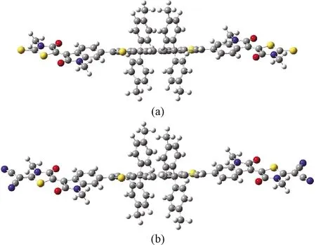
Fig.3 Molecular geometries of(a)WH1 and(b)WH7
2.2 Optical absorption spectroscopy and energy levels
The ultraviolet(UV)-vis absorption was used to determine the optical features of two molecules.Solution absorption spectra were measured from their chlorobenzene solutions with a concentration of 0.2 mg/mL.Thin films for absorption measurements were prepared via spin-casting from their chlorobenzene solutions with a concentration of 5 mg/mL.As shown in Fig.4(a), WH1 displays an absorption peak at 417 nm which is assigned to π-π*transition[29], and an absorption peak at 627 nm which is attributed to the intramolecular charge transfer(ICT)[30]from the center IDT donor unit to the two endcap acceptor units.For WH7, the π-π*transition peak locates at 425 nm while the ICT peak locates at 650 nm.Their solution absorption onsets were 703 nm for WH1 and 734 nm for WH7, respectively.The significantly red-shifted ICT peak and absorption onset of WH7 relative to WH1 was attributed to the enhanced electron push-pull effect in WH7 structure as four additional cyano groups have strong electron-withdrawing abilities.In thin film, WH1 shows a π-π*transition peak at 444 nm and ICT peak at 626 nm.In addition, there is a weak absorption shoulder(around 680 nm)that results in a significantly red-shifted absorption(onset: 758 nm)in comparison with the solution case.For WH7, the π-π*transition peak locates at 427 nm and ICT peak at 672 nm together with a weak absorption shoulder(around 700 nm)which significantly broaden the absorption profile and reduce the bandgap of the molecule.The film absorption onset is 808 nm.Both absorption shoulders in thin films indicate the well-ordered aggregated formation of WH1 and WH7 in the solid state[31].Their optical bandgaps were calculated from the crossover point of the normalized absorption and photoluminescence(PL)spectra[32].WH1 shows anEgoptof 1.65 eV and WH7 shows anEgoptof 1.57 eV.Generally, the short-wavelength absorption of D-A molecules is decided by the absorption of D unit, while the long-wavelength absorption is caused by ICT between D and A.The molecular structures of WH1 and WH7 are very similar, and the only difference is that the A unit of WH7 is cyano rhodanine, which has a stronger ability of electron-withdrawing.For WH1, the weak ICT has little difference between the solution and film, so ICT was hardly changed.In the film, the short wave makes the D unit stacking better, so the red-shift absorption happened.For WH7, the stronger ICT caused more difference in the film.Therefore, the ICT band has a red shift.
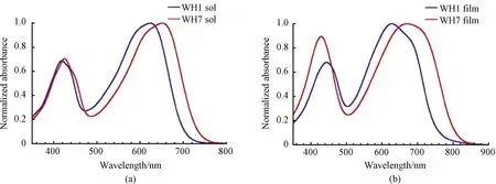
Fig.4 UV-vis spectra of WH1 and WH7 in(a)chlorobenzene solution(0.2 mg/mL);(b)thin film
Cyclic voltammetry was used to determine the ionization potential(IP)and electron affinity(EA)to give approximate values of orbital energy levels[33]by the equations ofEHOMO=-(4.8 +EIP);ELUMO=-(4.8 +EEA).As shown in Fig.5, for WH1, the IP is 0.60 eV and EA is-1.13 eV, and then the approximate HOMO and LUMO levels were estimated to be-5.40 eV and-3.67 eV.For WH7, the IP is 0.59 eV and EA is-1.02 eV, which give the estimation of HOMO and LUMO values about-5.39 eV and-3.78 eV, respectively.Absorption characteristics and energy levels are shown in Table 1.Similar to the case of ICT peak red-shifting in the absorption studies, the strong electron-withdrawing ability of CNRD in comparison to that of RD again dominates the low-lying LUMO level of WH7 relative to that of WH1 and further reduced the optical bandgap.
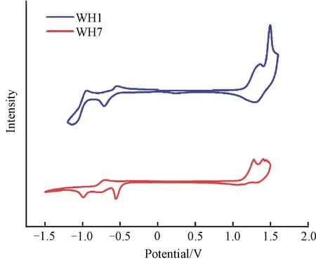
Fig.5 Cyclic-voltammetry measurements of WH1 and WH7 films

Table 1 Absorption characteristics and energy levels
2.3 Solar cells fabrication and performance
As shown in Table 2 and Fig.6(a), under the AM1.5 G condition, the optimal PBDB-T:WH1 devices give an averageJscof(5.04±0.40)mA/cm2, an averageVocof(0.95±0.01)V and an average of fill factor(FF)(53.4±2.4)%.Finally, PBDB-T:WH1 shows an average PCE of(2.58±0.29)% and the best PCE of 2.95%.For PBDB-T:WH7 devices, theVocdrops to(0.80±0.01)V, but bothJscand FF increase significantly, which are(11.70±0.17)mA/cm2and(66.5±1.3)%, respectively.Then the PCE of PBDB-T:WH7 increases to an average value of(6.24±0.20)% and the best value of 6.59%.For theJscdifference, one could clearly see the broad and great external quantum efficiency(EQE)response of WH7 device relative to WH1 device, as shown in Fig.6(b).The broad EQE of WH7 device could be attributed to the narrow bandgap of WH7, as WH7 could absorb more photons in the near IR region than WH1.For both PBDB-T:WH1 and PBDB-T:WH7 devices, the difference betweenJscfrom theJ-Vcharacterization and theJsccalculated from EQE was within 5%.To further understand theJscand FF differences, the mobility, recombination mechanism and morphology studies are discussed next.Besides, it is shown that theVocdifference(0.15 V)is greater than the LUMO level differences of WH1 and WH7(0.11 V)that measured by CV, which indicates the greater energy loss of WH7 device relative to that of WH1 device.The energy loss details would be also discussed in the later part.

Table 2 Solar cells performances of PBDB-T:WH1 and PBDB-T:WH7 devices under the optimal conditions
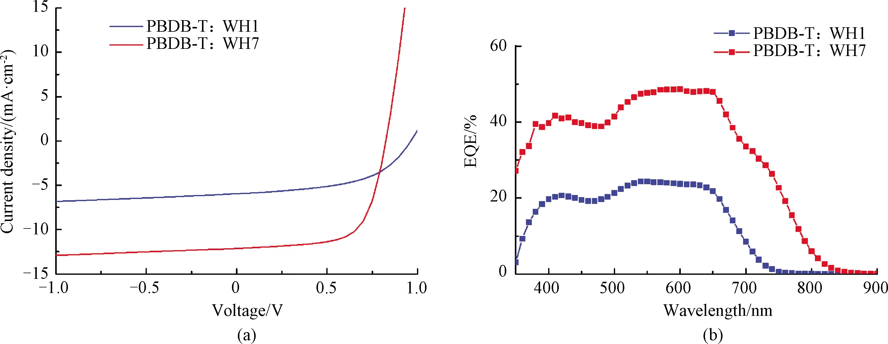
Fig.6 PBDB-T:WH1 and PBDB-T:WH7 devices:(a)J-V curves;(b)EQE curves
2.4 SCLC measurements
As shown in Fig.7(a), for PBDB-T:WH1, we obtain the hole mobilities of 2.6×10⁻⁴cm2/(V·s)(162 nm)and 3.8×10⁻⁴cm2/(V·s)(138 nm).For PBDB-T:WH7, the measured hole mobilities are 2.9×10⁻⁴cm2/(V·s)(195 nm)and 3.7×10⁻⁴cm2/(V·s)(141 nm).It is reasonable that both PBDB-T:WH1 and PBDB-T:WH7 active layers have a similar hole mobility level at the order of 10-4cm2/(V·s), as they have the same hole transport material of PBDB-T.And these hole mobility values are also consistent with the mobility reported in Ref.[34].For the electron mobility, as shown in Fig.7(b), the active layer of PBDB-T:WH1 gain the mobilities of 7.4×10⁻⁷cm2/(V·s)(164 nm)and 5.4×10⁻⁷cm2/(V·s)(107 nm).For PBDB-T:WH7, the measured mobilities are 3.9×10⁻⁵cm2/(V·s)(150 nm)and 6.3×10⁻⁵cm2/(V·s)(97 nm).The electron mobility of PBDB-T:WH7 is two orders of magnitude greater than that of PBDB-T:WH1.Nevertheless, the hole/electron transport is not balanced in both devices.PBDB-T:WH7 has a relatively close hole/electron transport characteristic and the FF is substantially greater than that of PBDB-T:WH1[35].
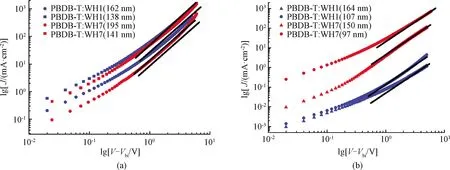
Fig.7 SCLC mobility measurements of PBDB-T:WH1 and PBDB-T:WH7:(a)hole-only device curves;(b)electron-only device curves
2.5 Light intensity dependence studies
To investigate the insight of charge recombination dynamics of two devices, we measured the variations ofJscas a function of light intensity[36].It is reported that the light intensity(P)ofJscin PSCs could be described as the following power relation ofJsc∝Pα.The deviation fromα=1 is typically attributed to the bimolecular recombination, space charge effects, and variations in mobility between the two carriers.As shown in Fig.8(a), both devices show clearly good linear dependence ofJscon light intensity.PBDB-T:WH1 device gains a relatively smallαof 0.87.Since the hole/electron transport is highly unbalanced in PBDB-T:WH1 device, space charge effect and variations in mobility between the two carriers should be considered as well as the bimolecular recombination.For PBDB-T:WH7 device, theαgoes up to 0.90, suggesting a significant bimolecular recombination effect between the two carriers.In summary, both devices are undesirable since theirαare not close to 1 enough.The unbalanced hole/electron transport and relatively low electron mobility in the active layer led to a significant bimolecular recombination effect, especially for PBDB-T:WH1 device[35].
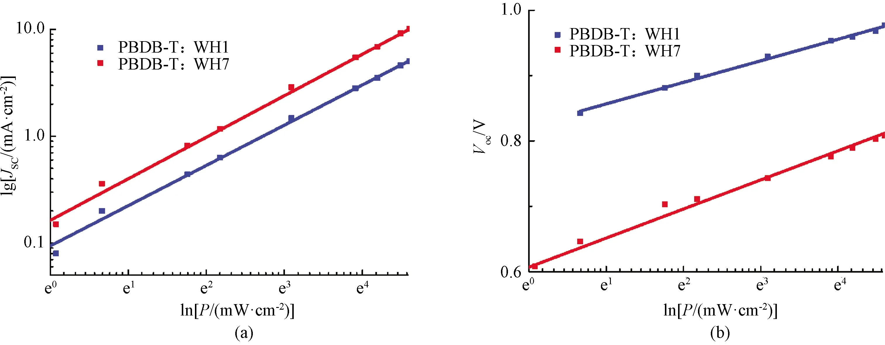
Fig.8 Light intensity dependence measurements of PBDB-T:WH1 and PBDB-T:WH7 devices:(a)Jsc-light intensity dependence;(b)Voc-light intensity dependence
For theVocand light intensity correlations[36], it is demonstrated that the light intensity dependence of theVoccan provide insight into the role of trap-assisted recombinationversusbimolecular recombination at open circuit, and follow the equation ofVoc∝nkT/qlnP, wherenis a constant,kis the Boltzmann′s constant,Tis the temperature,qis the elementary charge, andPis the incident light intensity.The slope of theVocvs.lnPgivesnkT/qfor bimolecular recombination and trap-assisted recombination competitions.The slope which is close tokT/qimplies that the bimolecular recombination dominated the device under the open circuit condition, while the slope close to 2kT/qsuggest that trap-assisted recombination plays a major role in the device.As shown in Fig.8(b), PBDB-T:WH1 and PBDB-T:WH7 devices show slope of 1.31kT/qand 1.76kT/q, respectively.It suggests that both bimolecular and trap-assisted recombination happen in both devices at open circuit, however, the bimolecular recombination is the major in PBDB-T:WH1 while trap-assisted recombination is the major in PBDB-T:WH7.
2.6 Morphology studies
Blend morphologies were probed by bright-field transmission electron microscopy(BF-TEM), and the results are provided in Fig.9.The bright regions in the BF-TEM images are assigned to the polymer donor phase while the dark regions are assigned to the acceptor phase according to their absorbing electron abilities’ difference.For both PBDB-T:WH1 and PBDB-T:WH7 shown in Figs.9(a)and(b), they are nearly indistinguishable from each other and that contain a continuous interpenetrating network of polymer phases with a domain size of 40-50 nm, which is at a decent scale for the charge separation[37].There are dark spots corresponding to WH1 shown in Fig.9(a)and WH7 shown in Fig.9(b), respectively.But their domain sizes are difficult to estimate due to lacking of contrast.Overall, the TEM studies shows that both PBDB-T:WH1 and PBDB-T:WH7 blend films have similar phase-separation and their different FF value could not be attributed to the phase-separation difference.
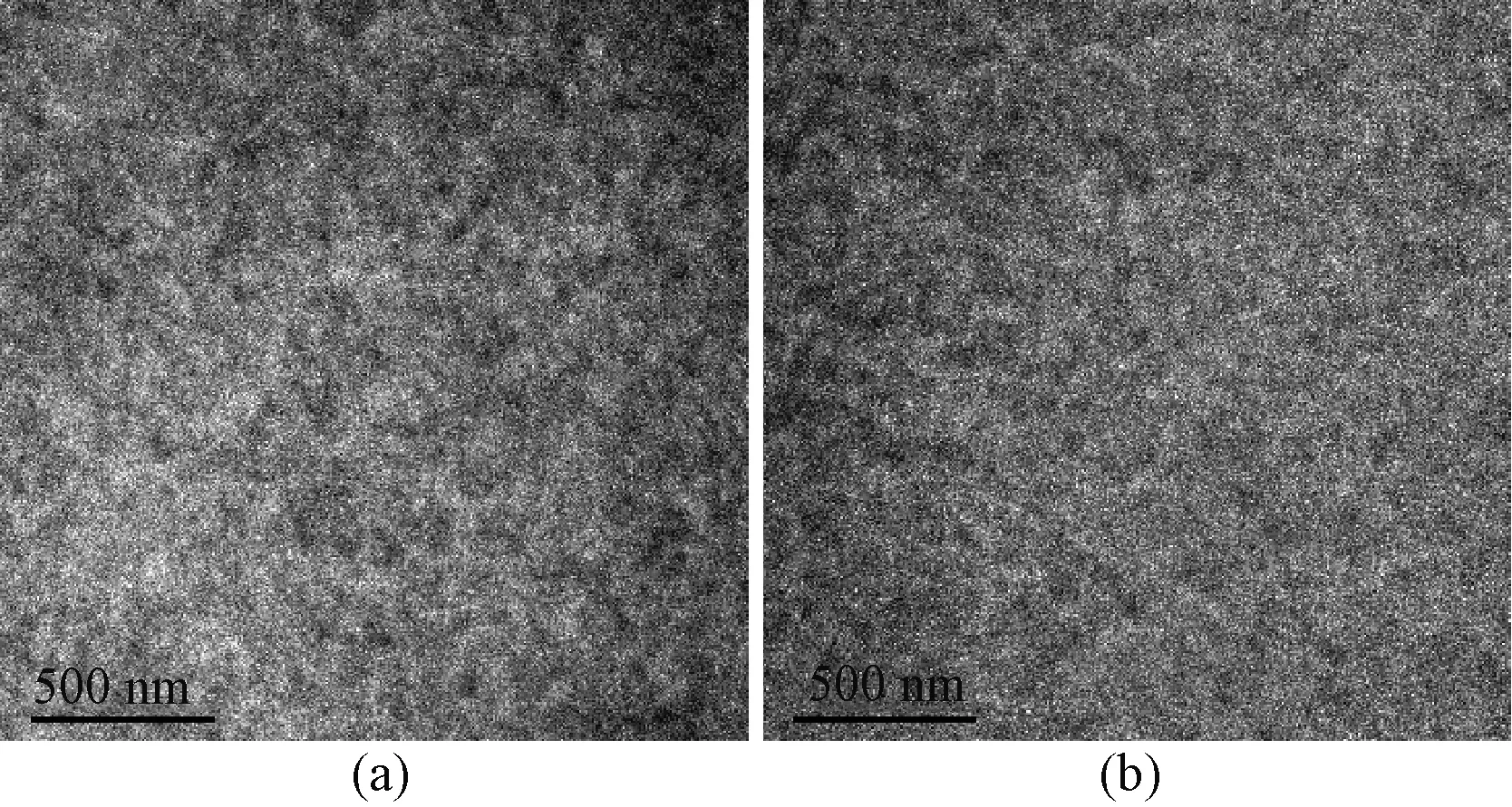
Fig.9 TEM images of active layers:(a)PBDB-T:WH1;(b)PBDB-T:WH7
2.7 Energy loss studies
To understand the insight of theVocdifference between PBDB-T:WH1 and PBDB-T:WH7 devices,ECTand energy loss analysis of the two devices were conducted on the basis of the sensitive EQE(sEQE)and electroluminescence(EL)spectra according to the reported method[38].As shown in Fig.10, theECTof PBDB-T:WH1 and PBDB-T:WH7 devices are estimated to be 1.51 eV and 1.45 eV, respectively, by fitting the low-energy band in the sEQE and EL spectra.The ΔECTis defined by the equation of ΔECT=Egopt-ECT,Egoptis the optical bandgap of WH1 or WH7 that represents the blend film since theirEgoptvalues are smaller than that of PBDB-T.Then ΔECTwas calculated to be 0.14 eV for PBDB-T:WH1 device and 0.12 eV for PBDB-T:WH7 device, respectively.The non-radiative energy loss(qΔVnr)is calculated by the EQE of EL(EQEEL)via the equation[39]qΔVnr=-kTln(EQEEL), whereqis the elementary charge,kis the Boltzmann’s constant, andTis the temperature, and theqΔVnrof 0.24 eV for PBDB-T:WH1 and 0.34 eV for PBDB-T:WH7 are provided, respectively, as shown in Figs.10(c)and(d).The total energy loss(Eloss)values of PBDB-T:WH1 and PBDB-T:WH7 devices were determined to be 0.70 eV and 0.77 eV, respectively, which are provided by the equation ofEloss=Egopt-qVoc(Vocis acquired from the average value in Table 2)[40].Since the totalElossconsists of three different parts[20,40],i.e.,Eloss=ΔECT+(qΔVr)+(qΔVnr),qΔVrcould be calculated to be 0.32 eV for PBDB-T:WH1 and 0.31 eV for PBDB-T:WH7, respectively.These values are summarized in Table 3, and the main factor of high energy loss in PBDB-T:WH7 device is due to the relatively greaterqΔVnr(0.34 eV)in comparison to that of PBDB-T:WH1(0.24 eV).

Table 3 Energy loss analysis of PBDB-T:WH1 and PBDB-T:WH7 devices
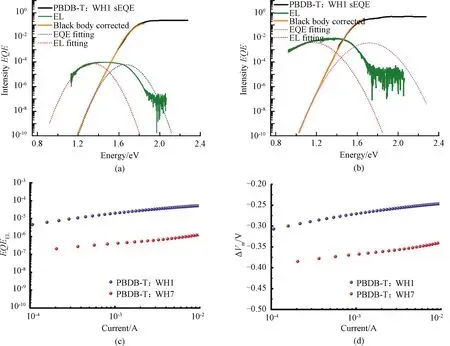
Fig.10 ECT measurements of PSC devices:(a)PBDB-T:WH1;(b)PBDB-T:WH7;(c)EQEEL measurements of PBDB-T:WH1 and PBDB-T:WH7;(d)ΔVnr measurements of PBDB-T:WH1 and PBDB-T:WH7
3 Conclusions
In summary, two A-D-A type acceptor molecules are designed by using the oxindole-based bridge unit to link the endcap A and the center D units.Two new acceptor molecules WH1 and WH7 have different end-groups showing different optical and energy properties.WH7 with the stronger electron-withdrawing end-group displayed a smaller bandgap and a lower-lying LUMO level relative to WH1.For PSC applications, PBDB-T:WH7 device gave largerJscand FF, but a smallerVocand finally exhibited the greater PCE in comparison to PBDB-T:WH1 device.Device mechanism studies showed that the narrow bandgap and greater electron mobility of WH7 relative to WH1 were the main reasons for achieving better performance.However, PBDB-T:WH7 device had a relatively large radiative energy loss(qΔVr)which limited its performance.This work shows that designing small molecular acceptors with the oxindole-based bridge is a facile strategy to couple the electron-deficient building blocks via the Knoevenagel condensation, which could tune the light absorption, energy levels, electron mobility and finally improve the device performance.
 Journal of Donghua University(English Edition)2022年3期
- Journal of Donghua University(English Edition)的其它文章
- Effects of Concentration of(3-Aminopropyl)Triethoxysilane on Waterborne Polyurethane
- Design of Creative Incentive Contract of Cultural and Creative Industry Chain from Dual Perspective
- PbI2/Pb5S2I6 van der Waals Heterojunction Photodetector
- Health Monitoring of Induction Motor Using Electrical Signature Analysis
- Acquisition, Pointing and Tracking System for Shipborne Space Laser Communication without Prior Information
- Students’ Feedback on Integrating Engineering Practice Cases into Lecture Task in Course of Built Environment
