
Gate tunable Rashba spin–orbit coupling at CaZrO3/SrTiO3 heterointerface
2022-06-29 08:56:10WeiMinJiang姜偉民QiangZhao趙強JingZhuoLing凌靖卓TingNaShao邵婷娜ZiTaoZhang張子濤MingRuiLiu劉明睿ChunLiYao姚春麗YuJieQiao喬宇杰MeiHuiChen陳美慧XingYuChen陳星宇RuiFenDou竇瑞芬ChangMinXiong熊昌民andJiaCaiNie聶家財
Chinese Physics B 2022年6期
關鍵詞:趙強
Wei-Min Jiang(姜偉民) Qiang Zhao(趙強) Jing-Zhuo Ling(凌靖卓) Ting-Na Shao(邵婷娜)Zi-Tao Zhang(張子濤) Ming-Rui Liu(劉明睿) Chun-Li Yao(姚春麗) Yu-Jie Qiao(喬宇杰)Mei-Hui Chen(陳美慧) Xing-Yu Chen(陳星宇) Rui-Fen Dou(竇瑞芬)Chang-Min Xiong(熊昌民) and Jia-Cai Nie(聶家財)
1Department of Physics,Beijing Normal University,Beijing 100875,China
2State Key Laboratory of Luminescence and Applications,Changchun Institute of Optics,Fine Mechanics and Physics,Chinese Academy of Sciences,Changchun 130033,China
Keywords: CaZrO3/SrTiO3,2DEG,Rashba spin–orbit coupling,gate voltage
1. Introduction
Owing to the rapid development of film technology,a large amount of oxide heterointerfaces among transition metal oxides (TMOs) have been fabricated intensively, exhibiting a lot of intriguing physical functionalities because of their unique electronic structure and properties.[1–10]One typical breakthrough was that the interface between two ABO3type perovskite insulators,e.g., LaAlO3and SrTiO3(LAO/STO), hosts a high-mobility two-dimensional electron gas (2DEG).[11]The conductive interface possesses quantities of fascinating properties such as ferromagnetism,[12–14]superconductivity,[15,16]and strong Rashba spin–orbit coupling (Rashba-SOC),[17]which results from the interfacial breaking of inversion symmetry.
Apart from the LAO/STO interface, 2DEGs have also been found in other STO-based systems.[18–24]In 2015,Chenet al.created a newly nonpolar interface in 3d strong correlated systems,CaZrO3/SrTiO3(CZO/STO).The critical thickness of CZO is 6 unit cell for the occurrence of interface conduction and it is much attractive via its high electron mobility more than 6×104cm2/(V·s)at low temperature,almost three times of the mobility of 2DEG at the LAO/STO interface.[25]Meanwhile,Niuet al.tuned the CZO/STO interface by using external ionic liquids(ILs)gating according to the electrolyte gate mechanism.[26]Besides, compared to the LAO/STO interface,the CZO/STO interface has a better lattice match and nonpolar property,which may have critical reference not only for the investigation of conductive mechanism but also for the study of diversified novel physical properties,such as Rashba-SOC,in CZO/STO system.
So far, however, the effect of the external gate voltage(VG)on the transport properties at the CZO/STO interface has not yet been systematically studied. In our work, the effects ofVGon the 2DEG transport properties at the CZO/STO interface,including Rashba-SOC,are studied. Our results show that tunable Rashba-SOC is susceptible to the externalVG.
2. Experimental details
CZO films with 22-unit-cells(~8.8 nm)were grown on(001)-oriented TiO2-terminated STO single-crystal substrates(5 mm×5 mm×0.5 mm with miscut less than 0.2°)by pulsed laser deposition(PLD)at 600°C in an oxygen atmosphere of~10-4mbar (1 bar=105Pa). During deposition, the repetition rate of laser pulse was 1 Hz and the fluence was 1.5 J/cm2(KrF laser,λ=248 nm). After deposition, the sample was cooled down to room temperature with a rate of 15°C/min without changing the oxygen pressure. The target-substrate distance was fixed at 5.6 cm.
The electrode contacts were made using Van der Pauw method by ultrasonic wire bonding(Al wire of 20 μm in diameter). All the transport properties were performed by a physical property measurement system(PPMS,Quantum Design)in the temperature range from 2 K to 300 K.The applied current for resistance measurements was 10 μA.TheVGwas applied to a back gate on the side of STO while the 2DEG was grounded. The leakage current was lower than 10 nA.
3. Results and discussion
To bring out the potential aspects of our 2DEG, a systematic investigation on gating effect is desirable. Figure 1(a)shows the schematic device structure. Figure 1(b) shows the sheet resistance (Rs) for the sample under different gate voltages at 2 K,Rsdecreases from~19579.35 Ω/□to~979.29 Ω/□asVGsweeps from-50 V to 100 V,reduced by a factor of 20. Figure 1(c)shows the Hall resistance measured at 2 K under different gate voltages from 0 to 9 T. AllRxy–Bcurves are well linear,signifying that there is only one species of charge carriers in the 2DEG. The collapse of theRxy–Bcurve with the increase ofVGidentifies the increase of the carrier density (ns). According to the formula,ns=-1/RHe,(eis the charge of an electron),nsis obtained. Actually, the tuning ability can be estimated asδn2D=ε0εrVG/t, whereε0is the vacuum permittivity,εrandtare the dielectric constant and the thickness of a dielectric material respectively.[27]Therefore, the required gate voltage is independent of CZO thickness. Figure 1(d)illustrates the carrier density as a function of the gate voltage. With theVGranging from-50 V to 100 V, thensat 2 K increases from~1.17×1013cm-2to~1.80×1013cm-2. Based on the data in Figs. 1(b) and 1(d),Hall mobility(μ)can be worked out. As charge carriers are accumulated,as shown in Fig.1(e),the gate voltage tunes the mobility from~27.29 cm2/(V·s) to~354.56 cm2/(V·s),increased by a factor of 13.

Another problem to be addressed is the gating effect of quantum interference, which is a unique characteristic of 2DEG. After gating 2DEG to the preset state, we measured the sheet resistance in the perpendicular magnetic field. Figure 2(a)shows the magnetoresistance(MR)at a fixed temperature of 2 K,defined byMR=[Rs(B)-Rs(B=0)]/Rs(B=0),as a function of magnetic field(B⊥interface)by applying various gate voltages. Two features can be identified from the data in Fig. 2(a). The first one is the occurrence of a sharp minimum atB=0 in allMR–Bcurves,which is a fingerprint of weak antilocalization owing to the Rashba-SOC.When the applied magnetic field is high enough,MRgrows smoothly,which is the classical orbital effect of the magnetic field. Secondly,forVG=0 and negative values,MRfirst grows and then decreases,i.e.the weak antilocalization and weak localization become weakened,respectively.

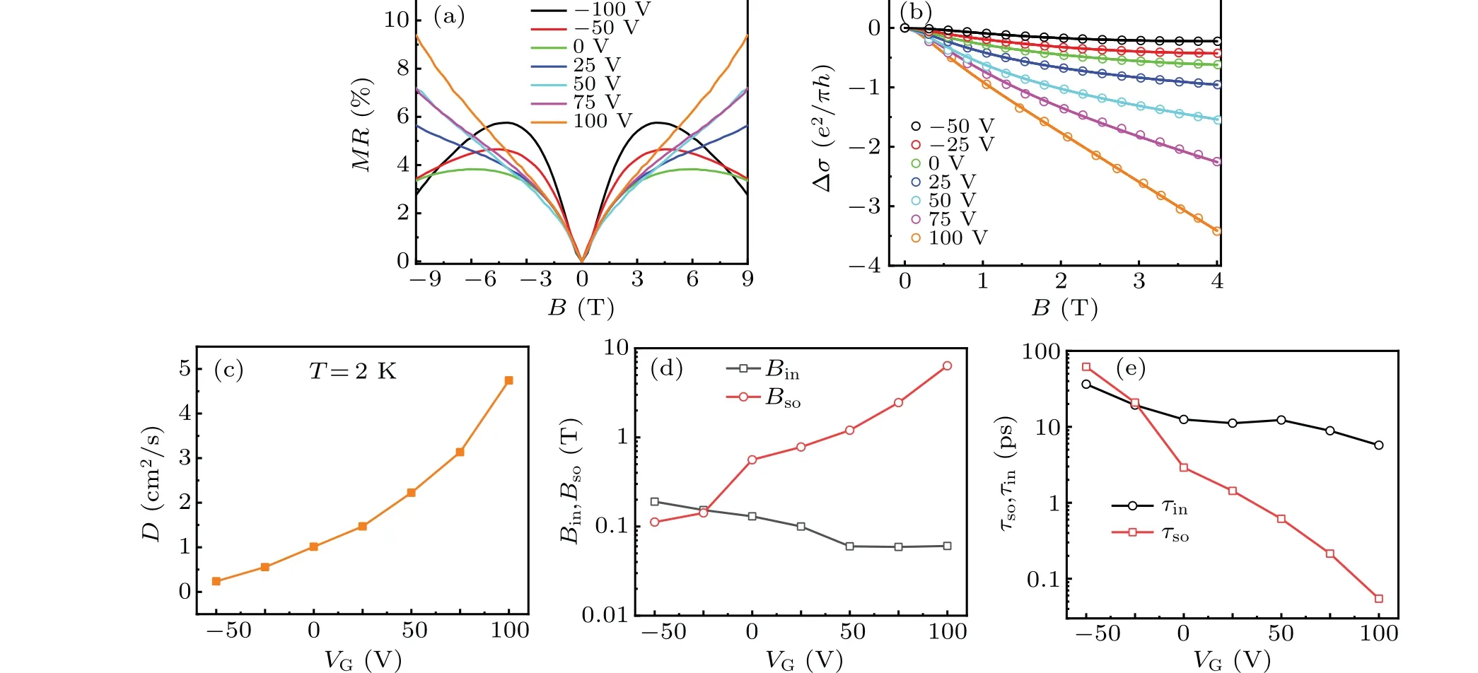
According to the results of the solid fitting curves in Fig.2(b),parameters(Bel,Bin,Bso)were obtained from the experimental results for the range of gate voltages from-50 V to 100 V.As shown in Fig.2(d),BsoandBinare well tuned byVG.Bsois the magnetic field related to the Rashba-SOC and it reflects on the SOC strength of 2DEG at CZO/STO interface.With theVGincreases,Bsoincreases from 0.112 T to 6.35 T.In other words,the strength of Rashba-SOC becomes stronger.Bindecreases from 0.19 T to 0.0605 T.The values ofBsoare in the same range as the ones reported previously for other STObased 2DEGs.[32–35]For negative gate voltages,Binis larger thanBsowhile atVG≥0 V,Bsois larger thanBinand increases monotonously withVG.
Similarly,the data ofτinandτsowithVGare also extracted on the basis of the fitting curves in Fig.2(e). With theVGincreases,τinranges from 36.41 ps to 5.72 ps,τsoranges from 61.76 ps to 0.054 ps, reduced by a factor of over three orders of magnitude. Rashba-SOC is dominant in this system.Furthermore,withVGincreases from-50 V to 100 V,the diffusion coefficientDincreases by 19.98 times, whileDof the LAO/STO interface 2DEG changes by only 2.5 times in the same gate voltage range.[32]Therefore, the effective regulation onτsowe observed results not only from the strong dependence ofBsoon the gate voltage, but also from the strong dependence ofDon the gate voltage.
Owing to the interfacial breaking of inversion symmetry, there is a potential gradient at the surface and interface,and electron SOC leads to band splitting, resulting in spinmomentum locking and spin-chirality opposite band structure(i.e.Rashba-SOC effect).[36]Rashba-SOC always exists in 2D systems such as LAO/STO,[11]CZO/STO,[25]LaVO3/STO,[9]and even amorphous LAO/STO,etc.[37,38]Its effect is expressed by the Bychkov–Rashba termHR=αR(k×?x)·σ,[39]
whereσare Pauli matrices,kis the wave vector,xis a unit vector along the electric filed direction,andαRis the Rashba parameter which measures the strength of the Rashba-SOC.Vazet al.determinedαRfrom the response of bilinear magnetoresistance in 2DEG at the LAO/STO interface.[40]They derived the dependence betweenVGandαR,and showed thatαRincreases monotonically withVGand reaches maximum at 120 V.
Furthermore,the corresponding Rashba spin splitting energyΔso=2kFαR(note thatkFis related tons, which is determined by Hall measurements, see the section below) is also determined, which ranges from 0.53 meV to 4.95 meV(Fig.3(b)). As can be seen clearly in Fig.3(b),the strength of Rashba-SOC at CZO/STO interface could be enhanced when applying positiveVGand becomes weakened when applying negativeVG. In a word, compared with the LAO/STO interface,[32]tunable Rashba spin–orbit coupling shows the similar gate dependence at the CZO/STO interface.
4. Conclusion
In summary,we demonstrate that Rashba-SOC of 2DEG at the nonpolar CZO/STO interface are well tuned by externalVG.Bsoincreases from 0.112 T to 6.35 T with the increase ofVGfrom-50 V to 100 V. Moreover, the mobility also increases from~27.29 cm2/(V·s)to~354.56 cm2/(V·s). More importantly,Dincreases by a factor of~19.98 andτsocan be strongly tuned which is reduced by a factor of over three orders of magnitude. Our results facilitate the development of more complex oxides heterointerfaces and provide new opportunities for designing electronic applications in traditional semiconductor devices.
Acknowledgement
Project supported by the National Natural Science Foundation of China (Grants Nos. 92065110, 11974048, and 12074334).
猜你喜歡
雜文選刊(2023年10期)2023-10-12 21:08:09
領導文萃(2023年13期)2023-07-10 11:47:23
Chinese Physics B(2022年6期)2022-06-29 08:54:16
Chinese Physics B(2021年10期)2021-10-28 07:20:10
民間文學(2019年10期)2019-11-21 21:36:10
東方藝術·書法(2018年1期)2018-04-30 00:33:58
愛你(2017年31期)2017-11-24 16:24:16
小說月刊(2017年8期)2017-08-16 20:33:29
微型小說選刊(2014年27期)2014-11-17 05:09:18
數(shù)學大世界·小學低年級輔導版(2009年3期)2009-04-14 04:37:58
- Chinese Physics B的其它文章
- Switchable terahertz polarization converter based on VO2 metamaterial
- Data-driven parity-time-symmetric vector rogue wave solutions of multi-component nonlinear Schr¨odinger equation
- Neutron activation cross section data library
- Multi-phase field simulation of competitive grain growth for directional solidification
- A novel similarity measure for mining missing links in long-path networks
- Effects of electrical stress on the characteristics and defect behaviors in GaN-based near-ultraviolet light emitting diodes