Secondary electron emission yield from vertical graphene nanosheets by helicon plasma deposition
Xue-Lian Jin(金雪蓮) Pei-Yu Ji(季佩宇) Lan-Jian Zhuge(諸葛蘭劍)Xue-Mei Wu(吳雪梅) and Cheng-Gang Jin(金成剛)
1School of Physical Science and Technology,Soochow University,Suzhou 215006,China
2Provincial Key Laboratory of Thin Films,Soochow University,Suzhou 215006,China
3Soochow University Analysis and Testing Center,Suzhou 215006,China
4Laboratory for Space Environment and Physical Sciences,Harbin Institute of Technology,Harbin 150001,China
The secondary electron emission yields of materials depend on the geometries of their surface structures.In this paper,a method of depositing vertical graphene nanosheet(VGN)on the surface of the material is proposed, and the secondary electron emission (SEE) characteristics for the VGN structure are studied. The COMSOL simulation and the scanning electron microscope(SEM)image analysis are carried out to study the secondary electron yield(SEY).The effect of aspect ratio and packing density of VGN on SEY under normal incident condition are studied. The results show that the VGN structure has a good effect on suppressing SEE.
Keywords: secondary electron emission, secondary electron yield, vertical graphene nanosheets, scanning electron microscope
1. Introduction
The secondary electron emission (SEE) is the emission that is yielded by the free electrons from a solid surface irradiated by external (also known as primary) electrons.[1]The secondary electrons consist of true secondary electrons and backscattered electrons. The true secondary electrons originate from the atoms of the target material surface and have energy values below 50 eV.The backscattered secondary electrons are primary electrons,which are yielded by either elastically or inelastically backscattering,and they have energy values between 50 eV and the primary electron energy.[2]In general,the total SEE of a surface is dominated by true secondary electrons.
The SEE is an important process in surface physics with applications in numerous fields,such as microchannel tube,[3]plasma display screen,[4]photomultiplier tube,[5]scanning electron microscope,[6]etc. The SEE can also adversely affect the applications and performance of devices,such as particle accelerator,[7]spacecraft surface,[8,9]fusion plasma,[10]RF/DC bias plasma process discharge,[11,12]Hall and spiral wave plasma thrusters,[13,14]etc. In plasma, strong SEE can significantly increase the electron heat flux from the plasma to the wall,resulting in(i)wall heating and wall evaporation,and(ii)plasma cooling and even extinction.The SEE from plasma bounding walls can be an undesired phenomenon.
The SEE is affected by material properties,[15,16]incident particle energy,[17–19]incident particle angle,[20]surface geometry and surface cleanliness as well.[21]The methods to suppress the SEE are based mainly on two factors, one is the surface material,[22–30]such as TiN film,[23]C film, graphite and graphene film,[24–30]and the other is the surface structure,[31–46]such as triangular and rectangular grooves,[36–38]microporous arrays,[39–42]velvet surfaces,[43–46]etc. Piviet al.[36]studied the reduction of the SEY of a grooved Cu surface, relating to the angle of triangular grooves and the aspect ratio and fraction of rectangular grooves. The aspect ratio is defined as the ratio of the height to the radius of the groove,and the fraction is the ratio of the radius to the spacing of grooves. Yeet al.[40]have studied the net SEY of a microporous Ag surface, which is reduced by 45%as compared with the SEY from a flat surface made from the same material. This was achieved by controlling the depth and relative placement of the pores with respect to each other.Swanson and Kaganovich[44]studied the carbon velvet material with higher aspect ratio, the SEY of which is reduced up to 65%as compared with a flat graphite surface.
The VGN structure has a similar geometry to microporous array, but is deposited on the surface like velvet. We assume that the structure can suppress the SEE of materials and investigate it. According to the reported research results,vertical graphene can be grown on different substrates,[47–50]and there are many ways to grow vertical graphene.[51]The vertical graphene used in this paper is grown on an Si (101)substrate by using the helical wave plasma chemical vapordeposition (HWP-CVD).[52]Because a thin graphite layer forms on the substrate surface during the deposition of vertical graphene,the role of the silicon substrate in the secondary electron emission process is negligible.
The COMSOL simulation and the SEM[2,53]image analysis method are used to study the SEY in this work. The effects of aspect ratio and packing density of VGNs on SEY under normal incident condition are studied.
2. Simulations
In the work the simulation is conducted by using the COMSOL_muiltiphysics_5.4.The simulation process is as follows. Firstly, a simulation model is created according to the geometric parameter under the geometry node. Secondly,the physical feild is set to be of charged particle tracing module,under which the attribute,number(N),direction and energy of the incident particles are set. the wall (represent the material surface)condition is set to be frozen, the secondary emission condition is set to be the probability, which is given by the interpolation function of the energy. The interpolation function is obtained from the Ref. [27]. The particle counter is used to count the number of particles leaving the surface of the material. The particle trajectories are plotted in the results branch. Finally,the number of particles(Ns)counted on a particle counter is calculate under the global evaluation node,and the secondary electron yield isδ=Ns/N.
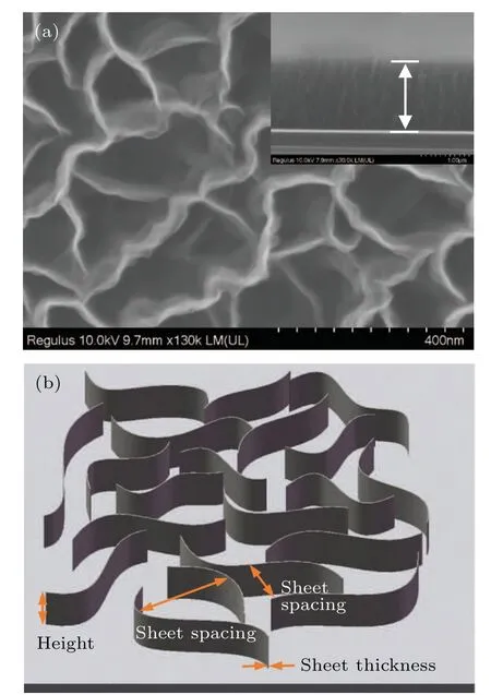
Fig.1. (a)SEM image of VGN surface structure,with inset showing crosssection, and double arrow marking packing height. (b)Schematic diagram of VGNs.[52]
The SEM image of VGNs is shown in Fig.1(a), and the schematic diagram is displayed in Fig.1(b).[52]It can be seen from Fig.1(b)that the geometric parameters of the model are height, thickness and sheet spacing of VGNs. Figure 1(a)shows that the geometry of VGNs is irregular,sheet spacing is not a definite value. The mean sheet spacing should be calculated. The curling of VGNs sheets results in a pore-like structure.We measure the multiple pore sizes and take their average value,which is the mean sheet spacing. The irregular geometric structure is reduced to a regular geometric structure during modeling. The SEM image shows that the structure formed by curled VGNs sheets contains obtuse angle and acute angle.The model is curved regularly by sinusoidal curve,the amplitude of the sinusoidal curve is about half of the mean sheet spacing and the array structure is arranged so that the structure of obtuse angle and acute angle can be obtained. This structure simplifies the model to a large extent and is close to the actual model. The model of VGNs constructed in COMSOL is shown in Fig.2.
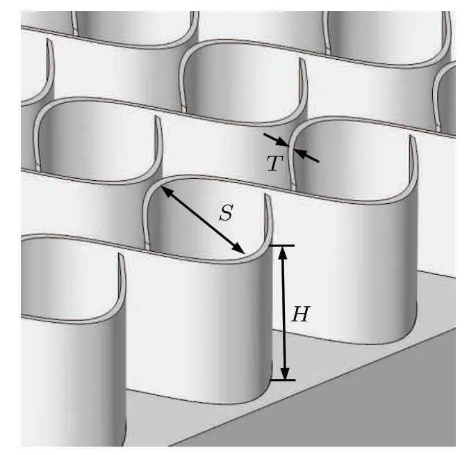
Fig.2. VGNs model constructed in COMSOL,with H,T,and S denoting height,thickness,and sheet spacing,respectively.
The incident particles are assumed to be electrons, the number of which is 5000, and their incident direction is assumed to be perpendicular to the sample substrate. Because the electric and magnetic fields can affect the incident electron beam and light spot, the whole simulation process is carried out without the electric field or the magnetic field. The diameter of the electron beam spot is 2000 nm. In this study the SEY of the sample at the primary electron energy between 20 eV and 1000 eV is discussed.The effects of aspect ratio and packing density of VGNs on SEY under normal incident condition are studied.The aspect ratio is defined as the ratio of the height of nanosheet to the mean sheet spacing(A=H/S). The packing density is defined as the ratio of the top surface area of VGN to the substrate area (P=st/ss,stis the top surface area,ssis the substrate area). Thestandsscan be obtained by measurements at the geometry node in COMSOL simulations. The geometric parameters of the VGN models are given in Table 1. The calculated values of aspect ratio (A) and the packing density(P)are also shown in the table.
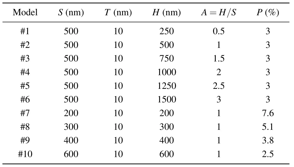
Table 1. Geometric parameters of VGNs models.
The influence of aspect ratio on SEY is studied by simulating the models#1–#6. And the influence of packing density on SEY is studied by simulating the models #2 and #7–#10.The results are shown in Figs.3 and 4.
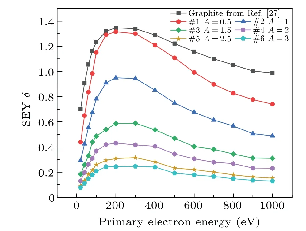
Fig.3. Curves of SEY versus primary electron energy from VGNs models(#1–#6 from Table 1), with aspect ratio A ranging from 0.5 to 3, primary energy varying from 20 eV to 1000 eV and SEY of planar graphite cited from Ref.[27](black filled squares)for comparison.
The SEYs of VGNs models with different aspect ratios are shown in Fig.3. The models#1–#6 have the same packing density of 3%, which means that the thickness and the sheet spacing remain the same, while the height varies with aspect ratio as shown in Table 1. The SEY variation trend of the simulation model is the same as that of the planar graphite from the literature. The yield first increases and then decreases with primary energy increasing. The SEY decrease withAincreasing in the whole energy range. The maximum value of SEY(δmax)is used to characterize the properties of secondary electron emission from material. Theδmaxof model #1 is 1.32,which is close to that of planar graphite(1.35). The slight reduction of SEY is due to the fact that model#1 has a height of 250 nm and a sheet spacing of 500 nm,leads to a low surface roughness,as indicated in the Caoet al.’s paper.[37]Caoet al.gave the following conclusion:for random rough surfaces with Gaussian statistics,slight roughness can increase the SEY and then the SEY decreases withRa(arithmetical mean roughness)increasing afterRahas gone beyond a certain level. Theδmaxof model#2 is about 0.95,which means a 30%reduction compared with that of planar graphite. And the model#3,#4,#5,#6 have the reduction of SEY by 57%,68%,76%,and 81%respectively as compared with graphite. The larger the value ofA,the better the suppression effect of SEE is. When the value ofAincreases, the decrement in magnitude ofδmaxSEY decreases,which means that the value of SEY cannot be reduced indefinitely. This resultaccords with the result of microporous array obtained by Yeet al.[40]
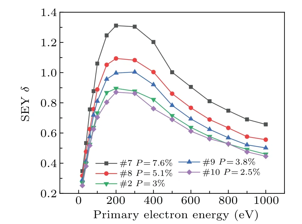
Fig.4. Curves of SEY versus primary electron energy from VGNs models(#2 and #7–#10 from Table 1), with packing density P ranging from 2.5%to 7.6%,and primary electron energy varying from 20 eV to 1000 eV.
The SEYs of VGN models with different packing densities are shown in Fig. 4. The models #2 and #7–#10 have the same aspect ratio of 1, which means the height and sheet spacing change with packing density as shown in Table 1. The SEY increases with packing density increasing. In this case,the largest value ofδmaxis 1.31 and the least value ofδmaxis 0.87,corresponding to the packing density 7.6%and 2.5%,respectively. The models with close packing density have close SEY values,for example,model#2 has theδmaxof about 0.89 and model#10 has theδmaxof about 0.87,and the two models have densities of 3%and 2.5%,respectively.The packing density of VGNs corresponds to the porosity of the microporous array, which is defined as the area of the pore to the area of the whole substrate surface. However, the change of packing density is opposite to that of porosity, which means that the higher the porosity, the smaller the packing density is. Thus,the result shown in Fig.4 accords with Yeet al.’s result about the porosities of microporous array.[40]
2.1. SEM analysis
The SEYs of two different VGNs samples are characterized by SEM,which are compared with the simulation results.The SEM test setup[2]is as follows. A planar graphite sample and two VGNs samples are introduced into the SEM vacuum chamber simultaneously. Scanning parameters such as spot size,working distance,brightness,contrast,current and magnification are kept consistent during the test. The scanningvoltages are 200,300,400,500,700,1000 V respectively,corresponding to the primary electron energy values of 200,300,400,500,700,1000 eV.The signal intensity of SEM detector is proportional to the number of secondary electrons collected,the pixels with black intensity indicate no SEE,and the pixels with white intensity indicate the highest SEE.The SEM image is decomposed into 8-bit pixel gray histogram with MATLAB,and the average value of pixel gray is calculated. The conversion factors between grayscale value and secondary electron emission yield at different voltages are calculated by using the pixel intensity calibration method of planar graphite. The graphite SEY parameters used for calibration are derived from the Isabel’s study.[27]
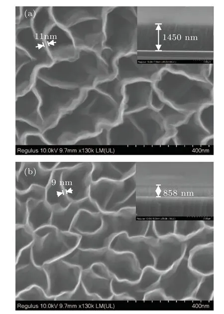
Fig.5. SEM image with structure parameter of(a)VG1 and(b)VG2.
The parameters of tow VGNs samples are shown in Table 2. The height, and thickness are obtained with the SEM image as shown in Fig.5. The mean sheet spacing is obtained by measuring the aperture several times and taking the average of these measurement values. The packing density is defined asP=((S+T)2?S2)/(S+T)2.These two VGN samples are named VG1 and VG2 respectively. The SEYs of two VGNs samples are finally calculated and plotted as shown in Fig.6.In order to make a comparison,the simulation models named#VG1 and #VG2 are established based on the parameters of these two samples. The simulation results are also shown in Fig.6.
It can be seen in Fig.6 that the SEY obtained by simulation is significantly lower than that by SEM analysis,because the wall of the simulation model is smoother and more uniform than the sample. The regular geometry is also the reason for the lower value obtained by simulation. According to the SEY trend line,the SEM analysis results have errors when the energy is greater than 500 eV.The SEYs of VGN samples are much smaller than that of graphite, indicating that the VGN has a good effect on suppressing SEE.The simulation results show that the SEY of #VG1 is smaller than that of #VG2.After eliminating various errors as shown in the error bar in Fig.6, we can conclude that the SEY of VG1 is smaller than that of VG2. This result accords with the simulation result.

Table 2. Parameters of two different VGNs samples.
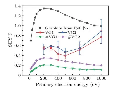
Fig.6. Curves of SEY versus primary electron energy of graphite(square)cited from Ref.[27],two VGNs samples(VG1(circle)and VG2(triangle))measured by SEM analysis,and two sample models(#VG1(rhombus)and#VG2(inverted triangle))obtained by simulation.
3. Summary
In this work,the packing density of VGNs structure corresponds to the porosity of the pore array. The packing densities studied range from 2.5%to 7.6%,implying porosities in a range from 92.4%to 97.5%.The porosities of pore array studied by Yeet al.[40]range from 0.1 to 0.7. This indicates that the VGN structure has a higher porosity. It is shown both in this paper and in Yeet al.’s study[40]that the higher the surface porosity,the smaller the SEY is,implying that VGN structure has its unique advantages in suppressing SEE.
In our previous research,[45]the whiskers on the velvet were about 3.5 microns in diameter and ranged in height from 0.5 mm to 3 mm, which can be recognized by bare eye. The thickness values of the VGN nanosheets studied in this paper are about 10 nm,and their heights range from several hundred to several thousand nanometers, and its size is smaller than that of the velvet structure. But its suppression of secondary electrons is as good as velvet’s.
The effects of aspect ratio and packing density of VGNs on SEY under normal incident condition are studied.The SEYvariation trend of the simulation model is the same as that of the planar graphite from the literature.The yield first increases and then decreases with primary energy increasing. And the SEY decreases withAincreasing in the whole energy range.WhenAincreases, the decreament in magnitude ofδmaxdecreases,which means that the value of SEY cannot be reduced indefinitely. The SEY increases with the augment of packing density. When the difference in packing density between two models is large, the difference inδmaxbetween them is large. Models with close packing density have close SEY values. The SEY of VGN sample obtained by SEM analysis is much smaller than that of graphite, and the sample with bigger aspect ratio and smaller packing density has a smallerδmaxvalue that accords well with the simulation value.
In conclusion, the simulation results and SEM analyses show that the VGN can suppress SEE,and the suppression effect is very good under the condition of high aspect ratio and low packing density.This study provides a scientific basis necessary for the research and development of a new technology of suppressing SEE.
Acknowledgements
Project supported by the National Natural Science Foundation of China(Grant No.11975163).The authors would like to thank Dr. Tan Haiyun for his suggestion for this work.
- Chinese Physics B的其它文章
- A broadband self-powered UV photodetector of a β-Ga2O3/γ-CuI p-n junction
- High-sensitive terahertz detection by parametric up-conversion using nanosecond pulsed laser
- High efficiency,small size,and large bandwidth vertical interlayer waveguide coupler
- High-fidelity resonant tunneling passage in three-waveguide system
- An analytical model for cross-Kerr nonlinearity in a four-level N-type atomic system with Doppler broadening
- Determine the physical mechanism and source region of beat wave modulation by changing the frequency of high-frequency waves

