Fullerene-based electrode interlayers for bandgap tunable organometal perovskite metal–semiconductor–metal photodetectors?
Wen Luo(羅文),Li-Zhi Yan(閆立志),Rong Liu(劉榮),Tao-Yu Zou(鄒濤隅),and Hang Zhou(周航)
School of Electronic and Computer Engineering,Peking University Shenzhen Graduate School,Shenzhen 518055,China
1.Introduction
Organolead halide perovskite materials(MAPbX3,MA is short for CH3NH3,X=I,Br or Cl)have attracted tremendous research efforts in the fields of solar cells,[1–3]photodetectors,[4,5]light-emitting diodes,[6]and lasers[7]inrecent years,due to their outstanding properties,such as ease of fabrication,high optical absorption coefficient,tunable optical bandgap,and long charge carrier diffusion length.[8–10]In particular,high gain and low noise perovskite photodetectors for ultraviolet(UV)/visible(Vis)light detections have been previously reported with comparable performance to silicon photodetectors.[11,12]It has been found that perovskite photodetectors are very sensitive to high energy x-ray photons,[13]with sensitivities outperforming their inorganic counterparts,such as a-Se and CdTeZn materials.
Conventionally,perovskite photodetectors are cataloged into three types:p–i–n photodiode,metal–semiconductor–metal(MSM)photoconductors,and phototransistors.For p–i–n perovskite photodiodes,electrode interlayers acting as a hole transporting layer or electron transporting layer are critical to the success of the device operation.For example,fullerenes derivatives phenyl-C61-butyric acid methyl ester(PCBM)are usually adopted in p–i–n type photodiode or solar cell device for electron extractions.[14,15]For MSM photodetectors made by inorganic semiconductors,such as silicon,the interlayer is less studied as a large electric field can be applied in these devices to overcome the Schottky barrier for carrier extractions.However,for the perovskite MSM device case,a large electric field will inevitably induce ion mobilization and material instability.[16]Even worse,MAPbX3materials are found to react with many metal electrodes,such as Ag,Al,and even Au,which further leads to large leakage current and device instability.[17]In fact the tunable bandgap of MAPbX3raises further considerations on the work function difference between metal and the semiconductor.It is,therefore,necessary to investigate the electrode interlayers to achieve highperformance stable MSM-type perovskite photodetector.[18,19]
In this study,a systematic investigation on how the fullerene-based electrode interlayers affect the MSM perovskite photodetector(Fig.1(a))performance has been conducted.Fullerenes derivatives are frequently used as electrontransporting layers(ETLs)in perovskite solar cells.[20,21]Here,we introduce two types of fullerene derivatives,i.e.,phenyl-C61-butyric acid methyl ester and indene-C60bisadduct(ICBA),as interfacial materials for the MSM per-ovskite photodetectors.The lowest unoccupied molecular orbital(LUMO)of the PCBM and the ICBA below the vacuum energy level has been previously reported to be 3.9 eV and 3.7 eV,respectively.[22,23]This is particularly interesting from the band alignment point of view,as the band gap of MAPb(I1?xBrx)3(0≤x≤1)can be continually adjusted from 1.5 eV(x=0)to 2.3 eV(x=1)with x ratio.As shown in Fig.1(b),the conduction band of the tunable bandgap perovskite may vary from~3.3 eV to~3.9 eV,[24,25]depending on the percentage of the Br substitution of I in the perovskite thin film.The charge transfer efficiency at the perovskite/PCBM or perovskite/ICBA interface has been evaluated by photoluminescence(PL)measurement and electrochemical impedance spectroscopy(EIS)measurement.
2.Materials and methods
2.1.Materials
PbI2was purchased from Alfa Aesar.CH3NH3I,PbBr2,and CH3NH3Br were purchased from Xi’an Polymer Light Technology Corp.PCBM and ICBA were purchased from Lumtec.To prepare the perovskite precursor solution,a 40-wt%solution of MAPbI3was synthesized by mixing PbI2and CH3NH3I in a 1:1 molar ratio in N,N-dimethylformamide(DMF).PbBr2and CH3NH3Br were dissolved in DMF at a 1:1 molar ratio with the concentration of 28.5 wt%denoted as MAPbBr3precursor.Solutions of 20 mg/mL of PCBM or ICBA were synthesized by dissolving PCBM or ICBA in 1,2-dichlorobenzene,respectively.All the solutions were heated at 70?C for 12 h inside a nitrogen- filled glove box.The desired MAPb(I1?xBrx)3(0≤ x≤ 1)precursors were made by stoichiometric mixing of MAPbI3and MAPbBr3precursors and stirred at 70?C for 1 h.
2.2.Device fabrication
Glass substrates(D-I001)were cleaned subsequently in deionized water,acetone,and ethanol in an ultrasonic bath for 15 min,followed by nitrogen flow drying.Then,the substrates were subjected to ultraviolet ozone treatment for 10 min before transferring to a glove box.The perovskite precursor solutions were spin-coated on the glass substrate at 3000 rpm for 40 s,with chlorobenzene anti-solvent treatment during the spin-coating process to slow down the crystallization speed of perovskite to achieve smooth compact thin films.[26]Next,the substrates were heated on a hot plate at 100?C for 10 min.The PCBM and ICBA solutions were then spin-coated on the substrate at 2000 rpm for 40 s.Finally,the Au electrode(50 nm)was thermally evaporated on the substrates via a shadow mask.The channel length ranges from 40μm to 100μm with the channel width/length ratio of ten.The effective area in our work ranges from 1.6×104μm2to 1×105μm2.
2.3.Device characterization
The scanning electron microscopy(SEM)images were obtained from a TESCAN field-emission SEM.The x-ray diffraction(XRD)pattern data was collected from a Bruker D8 advanced diffractometer with nickel- filtered Cu Kα radiation(1.5406A?)operating at 40 kV and 40 mA.The optical absorption of films was examined by UV–Vis absorption and transmission spectra(UV-2600,Shimadzu).The electrical characteristics of the photodetectors were tested using Agilent B1500 semiconductor parameter analyzer,equipped with a supercontinuum laser source(SC-PRO)and a wavelength selecting module(AOTF-Pro).Photoluminescence spectra were obtained using a 1-K series He–Cd laser.Electrochemical impedance spectroscopy measurement was conducted using an electrochemical workstation(CHI660E,Chenhua).
3.Results and discussion
A typical MAPbI3surface morphology is shown in Fig.1(c).The fabricated perovskite thin film is comprised of grains of several hundred nanometers,the size of which is similar to the perovskite film used in high-efficiency solar cells.The smooth thin film surface is beneficial for the formation of compact fullerenes layers via a spin coating technique.To determine the components of the perovskite,the x-ray diffraction patterns of the MAPbI3layers are shown in Fig.A1(a)in Appendix A.Moreover,UV–Vis absorption spectra of MAPbI3,ICBA,PCBM,MAPbI3/ICBA,and MAPbI3/PCBM films are given in Fig.A1(b).The spectral results confirm that the fullerenes layers have an insignificant contribution to the light absorption.
As shown in Fig.2(a),the color of MAPb(I1?xBrx)3changes from dark brown for MAPbI3(x=0)to yellow for MAPbBr3(x=1).All MAPb(I1?xBrx)3perovskite films are smooth and compact as shown in Fig.2(b).The SEM images in Fig.2(b)reveal that the morphology of perovskite thin film is significantly influenced by the I and Br ratio.As the Br content in MAPb(I1?xBrx)3increases,the perovskite thin film tends to form a high-quality MAPb(I1?xBrx)3film with a larger crystal size.The observation of larger grain size with increase Br content is consistent with previous reports,[30,31]which may be explained by the Ostwald ripening process.Figure2(c)exhibits a systematic shift of the absorption band edge to shorter wavelength with increasing Br content in MAPb(I1?xBrx)3.Meanwhile,the devices are measured under the wavelength of 500 nm in our research.Figure A3(a)exhibits x-ray diffraction patterns monitored in the 2θ range of 28?–31?for MAPb(I1?xBrx)3.The peak shifting towards larger diffraction angles suggests a decrease of the lattice constant,confirming the formation of I and Br hybrid perovskite.
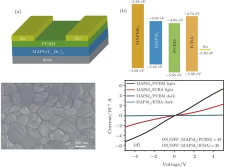
Fig.1.(a)Schematics of MAPb(I1?xBrx)3(0≤ x≤ 1)photodetector with fullerene-based interfacial layer.(b)Schematics of the energy diagram of perovskite,ICBA,and PCBM before contact.(c)The SEM image of the surface morphology of an MAPbI3thin film;the scale bar is 200 nm.(d)The I–V characteristics of devices in the dark and under light illumination at 500 nm with an intensity of 2 mW/cm2.
To investigate the influence of fullerene-based interlayers,perovskite photodetectors with different interlayers were measured under the dark and the illuminations condition.As shown in Fig.1(d),it is found that the MAPbI3photodetector with the PCBM interlayer exhibits higher photocurrent than the device with ICBA interlayer.Moreover,the photocurrent of the device with interlayer is about one order of magnitude larger than the device without interlayer as shown in Fig.A2(a).On the other hand,the channel length will significantly influence the responsibility,as revealed in Fig.A2(b).For photodetector based on PCBM and ICBA interface layer,as the channel length increases,the responsibility increases.Moreover,the device with PCBM interlayer has higher responsivity,achieving a responsivity of 100.8 mA/W when the channel length is 40μm,which is comparable to the previously reported perovskite photoconductor.[27–29]For different channel lengths,the device with PCBM interlayer has higher responsivity,achieving a responsivity of 100.8 mA/W when the channel length is 40μm(Fig.A2(b)).This could be attributed to better alignment between the conduction band of MAPbI3and the LUMO level of the PCBM,which facilitates the photo-generated electron extraction at the MAPbI3/PCBM interface.In contrast,there is a barrier of about 0.19 eV at the MAPbI3/ICBA interface.It is worth noting that photodetectors with fullerene-based interlayer give a similar dark current level,which is~1 nA when biased at 5 V.
The photocurrent of MAPb(I1?xBrx)3/fullerenes photodetectors is shown in Fig.2(d).The photocurrent is measured under an illumination intensity of 2 mW/cm2at 500 nm and under 5-V bias. The photocurrent decreases gradually as the Br content increases in MAPb(I1?xBrx)3,which is consistent with the trend of light absorption coefficient shown in Fig.A3(b). The inserted table in Fig.A3(b)presents the absorptivity changes from 0.0218 nm?1(x=0)to 0.0074 nm?1(x=1). While all the photocurrents of MAPb(I1?xBrx)3/fullerenes photodetectors decrease as the Br content increases,the photocurrent of photodetectors with PCBM interlayer decreases faster than that with ICBA interlayer.As a result,the photodetectors with ICBA interlayer exhibit larger photocurrent than that with PCBM interlayer when x is larger than 0.8.
Accordingly,the responsibility R is the generated photocurrent per unit power of the incident light on the effective area and can be expressed as(Ip?Id)/PoptS,where Ipis the photocurrent,Idis the dark current,Poptis the incident-light intensity,and S is the effective illuminated area.[32,33]The specific detectivity D?is the ability of a detector to detect weak optical signals and can be estimated from A1/2R/(2qId)1/2,where A is the effective area of the device,q is the electronic charge,and R is the responsivity.[32,33]The responsivity and specific detectivity of the photodetectors at different Br contents are calculated and shown in Fig.2(e).The responsiv-ity of the MAPb(I1?xBrx)3/ICBA photodetector has become slightly higher than that of MAPb(I1?xBrx)3/PCBM photodetector when x is lager than 0.8.
Remarkably,it is worth noting that the specific detectivity of MAPb(I1?xBrx)3/ICBA has become much higher than that of MAPb(I1?xBrx)3/PCBM when x is larger than 0.6.This fact suggests that the ICBA interlayer could help to effectively extract the photogenerated electrons while maintaining a sufficient low dark current in the wide bandgap perovskite photodetector.The ON/OFF ratio of the MAPb(I1?xBrx)3/ICBA and MAPb(I1?xBrx)3/PCBM photodetectors is plotted in Fig.2(f),which also shows a turning around x=0.6 where the ICBA interlayer provides the device with a higher ON/OFF ratio.

Fig.2.(a)Photographs of three-dimensional(3D)MAPb(I1?xBrx)3(0≤x≤1) films on glass substrates.(b)The SEM images of MAPb(I1?xBrx)3 films;the scale bar is 200 nm.(c)The absorbance of the MAPb(I1?xBrx)3 films.The dotted line represents the illumination wavelength(500 nm)in our measurement.(d)Photocurrent of MAPb(I1?xBrx)3(0≤ x≤ 1)/fullerenes photodetectors when biased at 5 V under light illumination at 500 nm with an intensity of 2 mW/cm2.(e)Responsivity and specific detectivity and of MAPb(I1?xBrx)3/fullerenes photodetectors.(f)ON/OFF ratio of MAPb(I1?xBrx)3/fullerenes photodetectors.
We further investigate the transient response of photodetectors with PCBM and ICBA as electrode interlayers to a500-nm incident light with a light intensity of 2 mW/cm2at 5 V.In Fig.3(a),the photodetector with PCBM as the electrode interlayer shows a stronger photoresponse to incident light with a steady photocurrent of~ 5×10?8A,which is almost 2.5 times larger than that with ICBA as the electrode interlayer,in which the steady photocurrent is~2×10?8A.Figure 3(b)reveals the fast photoresponse of the photodetector to incident light with a rise time of<25 ms and a fall time of<50 ms,which is limited by our measurement equipment.
To examine the carrier extraction efficiencies of different fullerene-based materials,the photoluminescence spectra are measured and presented in Fig.4.The PL intensity of perovskite is quenched after the deposition of the fullerenes layer,indicating an effective charge transfer from perovskite to fullerenes layer.The quenching efficiency of luminescence in ICBA interlayered MAPbBr3device is higher than that of PCBM interlayered device(Fig.4(a)),in contrast to that of MAPbI3-based luminescence(Fig.4(b)).

Fig.3.(a)Transient response of photodetectors with different fullerenebased interfacial layers to a 500-nm incident light with a light intensity of 2 mW/cm2at 5 V.(b)Photocurrent rise and fall time of the devices.
The Ecof MAPbBr3perovskite is?3.3 eV,[34]while the LUMO for ICBA and PCBM is?3.7 eV[35]and?3.9 eV[36]respectively,which indicates that the ICBA may serve as a more suitable interlayer for MAPbBr3perovskite to efficiently transfer photogenerated electron,due to the energy level matching at interfaces between the ICBA and MAPbBr3perovskite.In contrast,Ecof MAPbI3perovskite is?3.9 eV;[34]thus,the PCBM becomes a better choice as the electron transport for MAPbI3.It has been previously reported that the corresponding Ecof MAPb(I1?xBrx)3is?3.9 eV,?3.6 eV,and?3.3 eV,[34]respectively,for the x value of 0,0.33,and 1.This implies that when the ratio of Br is over 0.33,the LUMO level of the ICBA gets closer to Ecof the perovskite than that of PCBM.[34]
To further investigate the charge transport and recombination of perovskite photodetectors with different fullerenes interlayers,the electrochemical impedance spectroscopy of perovskite/fullerenes photodetectors was carried out under a dark condition with a sandwich structure(indium–tin–oxide(ITO)/perovskite/PCBM or ICBA/Au)measured with a bias of?1 V.[37–39]Meanwhile,the effective measurement area of our device is0.04cm2.The EIS is a technique for investigating the interfacial charge transfer properties of the photovoltaic cell.The equivalent circuit model is similar to other reports with p–i–n structure.[40]The results are shown in the Nyquist plot,the real component(Z0)is the abscissa axis and the imaginary part(Z00)is the vertical axis.The data is fitted into an equivalent circuit,as shown in the illustration in Fig.4(c).In the model circuit,the series resistance Rsrepresents the contact resistance from both electron and hole transport layers.The low-frequency arc in the Nyquist plots is associated with the recombination resistance,in parallel with a chemical capacitance.[41]As the results shown in Fig.4(c),Rrecof MAPbBr3/PCBM is 1.5×10³? and Rrecof MAPbBr3/ICBA is 8.9×10³?.The larger Rrecsuggests the suppression of recombination of electron and hole due to efficient carrier extraction.Meanwhile,as shown in Fig.4(d),MAPbI3/PCBM is larger than MAPbI3/ICBAonRrec,which indicates that PCBM is more suitable for MAPbI3/fullerenes photodetector.These results agree with photoluminescence.
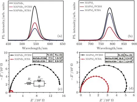
Fig.4.(a)Comparison of photoluminescence spectra of MAPbBr3,MAPbBr3/ICBA,and MAPbBr3/PCBM.(b)Comparison of photoluminescence spectra of MAPbI3,MAPbI3/ICBA,and MAPbI3/PCBM.(c)Electrochemical impedance spectroscopy of MAPbBr3/fullerenes photodetector;the illustration shows the equivalent circuits of perovskite/fullerenes photodetector.(d)Electrochemical impedance spectroscopy of MAPbI3/fullerenes photodetector under a dark condition.
4.Conclusions
In summary,we have proposed a strategy to enhance the performance of organometal perovskite photodetector by using interlayers to improve the charge injection at the metal/organic interface. The MAPbI3photodetector with PCBM interlayer demonstrates much better performance than that with ICBA interlayer,reaching a responsivity of 100.8 mA/W.We have also demonstrated that the photocurrent of MAPb(I1?xBrx)3/fullerenes decreases as the Br content increases,and the MAPb(I1?xBrx)3photodetector with ICBA interlayer exhibits better performance compared to that with PCBM interlayer when x is no less than 0.8.To illustrate these results,accumulation and transport of carriers of the perovskite devices with two fullerene-based interlayers are investigated by PL spectra and EIS.We find that it is easier for carriers to transport and more difficult for exciton to recombine for MAPbBr3photodetector with ICBA interlayer compared to that with PCBM interlayer,which is opposite in MAPbI3/fullerenes photodetector.
Appendix A
The following figures show the x-ray diffraction patterns,photocurrent of the devices,and the absorptivity of MAPb(I1?XBrX)3films.
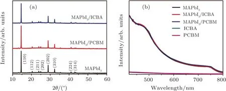
Fig.A1.(a)XRD patterns of MAPbI3,MAPbI3/PCBM,and MAPbI3/ICBA.(b)The absorbance of the MAPbI3and MAPbI3/fullerenes layers.
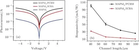
Fig.A2.(a)Photocurrent of the device with and without fullerenes interlayer.(b)The responsivity of the MAPbI3/fullerenes devices with different channel lengths.
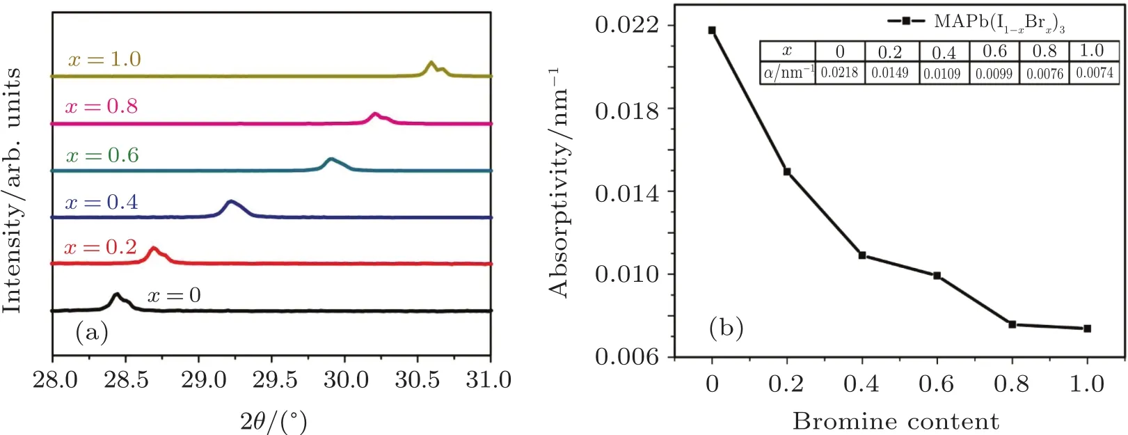
Fig.A3.(a)XRD patterns of MAPb(I1?xBrx)3magnified in the region of 2θ =28?–31?.(b)The absorptivity of MAPb(I1?xBrx)3 films.
[1]Jeon N J,Na H,Jung E H,Yang T Y,Lee Y G,Kim G,Shin H W,Il Seok S,Lee J and Seo J 2018 Nat.Energy 3 628
[2]Yang W S,Park B W,Jung E H,Jeon N J,Kim Y C,Lee D U,Shin S S,Seo J,Kim E K,Noh J H and Seok S I 2017 Science 356 1376
[3]Arora N,Dar M I,Hinderhofer A,Pellet N,Schreiber F,Zakeeruddin S M and Gratzel M 2017 Science 358 768
[4]Zhou J and Huang J 2018 Adv.Sci.5 1700256
[5]Luan S Z,Wang Y C,Liu Y T and Jia R X 2018 Chin.Phys.B 27 47208
[6]Wei Y,Cheng Z and Lin J 2018 Chem.Soc.Rev.48 310
[7]Zhu H,Fu Y,Meng F,Wu X,Gong Z,Ding Q,Gustafsson M V,Trinh M T,Jin S and Zhu X Y 2015 Nat.Mater.14 636
[8]Jr P C,Savenije T J,Abdellah M,Zheng K,Yartsev A,Pascher T,Harlang T,Chabera P,Pullerits T and Stepanov A 2014 J.Am.Chem.Soc.136 5189
[9]Jin H H,Sang H I,Noh J H,Mandal T N,Lim C S,Chang J A,Yong H L,Kim H J,Sarkar A and Nazeeruddin M K 2009 Nat.Photon.7 486
[10]Burschka J,Pellet N,Moon S J,Humphrybaker R,Gao P,Nazeeruddin M K and Gr¨azel M 2013 Nature 499 316
[11]Dou L,Yang Y,You J,Hong Z,Chang W H,Gang L and Yang Y 2014 Nat.Commun.5 5404
[12]Dong R,Fang Y,Chae J,Dai J,Xiao Z,Dong Q,Yuan Y,Centrone A,Zeng X C and Huang J 2015 Adv.Mater.27 1912
[13]Gill H S,Elshahat B,Sajo E,Kumar J,Kokil A,Zygmanski P,Li L and Mosurkal R 2014 APS March Meeting
[14]Liu M,Johnston M B and Snaith H J 2013 Nature 501 395
[15]Docampo P,Ball J M,Darwich M,Eperon G E and Snaith H J 2013 Nat.Commun.4 2761
[16]Yuan H,Debroye E,Janssen K,Naiki H,Steuwe C,Lu G,Moris M,Orgiu E,Ujii H and Schryver F D 2016 J.Phys.Chem.Lett.7 561
[17]Sanehira E M,Schulz P,Reese M O,Ferrere S,Zhu K,Lin L Y,Berry J J and Luther J M 2016 ACS Energy Lett.1 38
[18]Chen S,Teng C,Zhang M,Li Y,Xie D and Shi G 2016 Adv.Mater.28 5969
[19]Wang Y,Yang D,Zhou X,Alshehri S M,Ahamad T,Vadim A and Ma D 2017 Org.Electron.42 203
[20]Nie W,Tsai H,Asadpour R,Blancon J C,Neukirch A J,Gupta G,Crochet J J,Chhowalla M,Tretiak S and Alam M A 2015 Science 347 522
[21]Seo J,Park S,Kim Y C,Jeon N J,Noh J H,Yoon S C and Sang I S 2014 Energy Environ.Sci.7 2642
[22]He Y,Chen H Y,Hou J and Li Y 2010 J.Am.Chem.Soc.132 1377
[23]Yoshida H 2014 J.Phys.Chem.C 118 24377
[24]Wang B,Xiao X and Chen T 2014 Nanoscale 6 12287
[25]Yusoff A R and Nazeeruddin M K 2016 J.Phys.Chem.Lett.7 851
[26]Salim T,Sun S,Abe Y,Krishna A,Grimsdale A C and Lam Y M 2015 J.Mater.Chem.A 3 8943
[27]Saraf R and Maheshwari V 2018 ACS Appl.Mater.Interfaces 10 21066
[28]Hu X,Zhang X,Liang L,Bao J,Li S,Yang W and Xie Y 2014 Adv.Funct.Mater.24 7373
[29]Tian W,Zhou H and Li L 2017 Small 13 1702107
[30]Loryuenyong V,Khiaokaeo N,Koomsin W,Thongchu S and Buasri A 2018 Micro&Nano Lett.13 486
[31]Yang M,Zhang T,Schulz P,Li Z,Li G,Kim D H,Guo N,Berry J J,Zhu K and Zhao Y 2016 Nat.Commun.7 12305
[32]Zeng L H,Wu D,Lin S H,Xie C,Yuan H Y,Lu W,Lau S P,Chai Y,Luo L B,Li Z J and Tsang Y H 2019 Adv.Funct.Mater.29 1806878
[33]Zeng L H,Lin S H,Li Z J,Zhang Z X,Zhang T F,Xie C,Mak C H,Chai Y,Lau S P,Luo L B and Tsang Y H 2018 Adv.Funct.Mater.28 1705970
[34]Wang B,Xiao X and Chen T 2014 Nanoscale 6 12287
[35]He Y,Chen H Y,Hou J and Li Y 2010 J.Am.Chem.Soc.132 1377
[36]Yoshida H 2014 J.Phys.Chem.C 118 24377
[37]Wang H,Wang Y,Bo H,Li W,Sulaman M,Xu J,Yang S,Yi T and Zou B 2016 ACS Appl.Mater.Interfaces 8 18526
[38]Juarezperez E J,Wuβler M,Fabregatsantiago F,Lakuswollny K,Mankel E,Mayer T,Jaegermann W and Morasero I 2014 J.Phys.Chem.Lett.5 680
[39]Wang P,Zhang J,Chen R,Zeng Z,Huang X,Wang L,Xu J,Hu Z and Zhu Y 2017 Electrochimica Acta 227 180
[40]Pockett A,Eperon G E,Peltola T,Snaith H J,Walker A,Peter L M and Cameron P J 2015 J.Phys.Chem.C 119 3456
[41]Christians J A,Fung R C and Kamat P V 2014 J.Am.Chem.Soc.136 758
- Chinese Physics B的其它文章
- Entangled multi-knot lattice model of anyon current?
- Miniature quad-channel spin-exchange relaxation-free magnetometer for magnetoencephalography?
- Observing the steady-state visual evoked potentials with a compact quad-channel spin exchange relaxation-free magnetometer?
- Quantum interferometry via a coherent state mixed with a squeezed number state?
- Cavity enhanced measurement of trap frequency in an optical dipole trap?
- 7.6-W diode-pumped femtosecond Yb:KGW laser?

